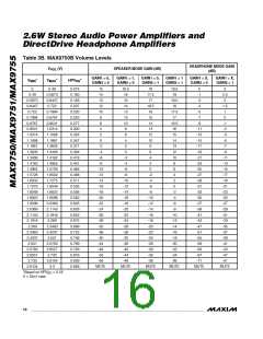
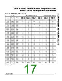
2.6W Stereo Audio Power Amplifiers and
DirectDrive Headphone Amplifiers
Table 4. Suggested Capacitor Manufacturers
SUPPLIꢀR
Taiyo Yuden
TDK
PHONꢀ
FAX
WꢀBSITꢀ
800-348-2496
807-803-6100
847-925-0899
847-390-4405
www.t-yuden.com
www.component.tdk.com
Thermal-overload protection limits total power dissipa-
tion in these devices. When the junction temperature
exceeds +160°C, the thermal-protection circuitry dis-
ables the amplifier output stage. The amplifiers are
enabled once the junction temperature cools by 15°C.
This results in a pulsing output under continuous ther-
mal-overload conditions as the device heats and cools.
1
f
=
−3DB
2πR C
IN IN
R
is the amplifier’s internal input resistance value
IN
given in the Electrical Characteristics. Choose C such
IN
that f
Setting f
is well below the lowest frequency of interest.
-3dB
too high affects the amplifier’s low-fre-
-3dB
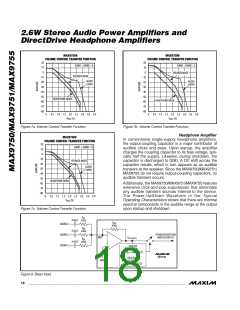
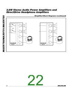
Output Power (Headphone Amplifier)
The headphone amplifiers have been specified for the
worst-case scenario—when both inputs are in phase.
Under this condition, the drivers simultaneously draw
current from the charge pump, leading to a slight loss in
quency response. Use capacitors with low-voltage
coefficient dielectrics, such as tantalum or aluminum
electrolytic. Capacitors with high-voltage coefficients,
such as ceramics, may result in increased distortion at
low frequencies.
headroom of V . In typical stereo audio applications,
SS
BIAS Capacitor
the left and right signals have differences in both magni-
tude and phase, subsequently leading to an increase in
the maximum attainable output power. Figure 10 shows
the two extreme cases for in and out of phase. In reality,
the available power lies between these extremes.
BIAS is the output of the internally generated DC bias
voltage. The BIAS bypass capacitor, C
, improves
BIAS
PSRR and THD+N by reducing power supply and other
noise sources at the common-mode bias node, and
also generates the clickless/popless, startup/shutdown
DC bias waveforms for the speaker amplifiers. Bypass
BIAS with a 1µF capacitor to GND.
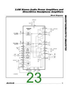
Power Supplies
The MAX9750/MAX9751/MAX9755 have different sup-
plies for each portion of the device, allowing for the opti-
mum combination of headroom and power dissipation
and noise immunity. The speaker amplifiers are pow-
Charge-Pump Capacitor Selection
Use capacitors with an ESR less than 100mΩ for opti-
mum performance. Low-ESR ceramic capacitors mini-
mize the output resistance of the charge pump. For
best performance over the extended temperature
range, select capacitors with an X7R dielectric. Table 4
lists suggested manufacturers.
ered from PV . PV
ranges from 4.5V to 5.5V. The
DD
DD
headphone amplifiers are powered from HPV
and
DD
V
. HPV
is the positive supply of the headphone
SS
DD
amplifiers and ranges from 3V to 5.5V. V is the nega-
SS
tive supply of the headphone amplifiers. Connect V to
SS
DD
CPV . The charge pump is powered by CPV
.
SS
Flying Capacitor (C1)
The value of the flying capacitor (C1) affects the load
regulation and output resistance of the charge pump. A
C1 value that is too small degrades the device’s ability
to provide sufficient current drive, which leads to a loss
of output voltage. Increasing the value of C1 improves
load regulation and reduces the charge-pump output
resistance to an extent. See the Output Power vs.
Charge-Pump Capacitance and Load Resistance
graph in the Typical Operating Characteristics. Above
2.2µF, the on-resistance of the switches and the ESR of
C1 and C2 dominate.
CPV
ranges from 3V to 5.5V and should be the same
DD
potential as HPV . The charge pump inverts the volt-
DD
age at CPV , and the resulting voltage appears at
DD
CPV . The remainder of the device is powered by V
.
SS
DD
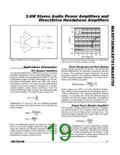
Component Selection
Input Filtering
The input capacitor (C ), in conjunction with the ampli-
IN
fier input resistance (R ), forms a highpass filter that
IN
removes the DC bias from an incoming signal (see the
Typical Application Circuit). The AC-coupling capacitor
allows the amplifier to bias the signal to an optimum DC
level. Assuming zero source impedance, the -3dB point
of the highpass filter is given by:
20 ______________________________________________________________________________________

 MAXIM [ MAXIM INTEGRATED PRODUCTS ]