2.6W Stereo Audio Power Amplifiers and
DirectDrive Headphone Amplifiers
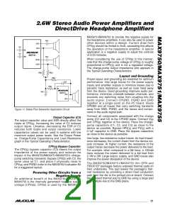
1000
V
DD
= 5V
R = 16Ω
L
100
10
A = 3dB
V
V
+1
-1
OUT(P-P)
OUTPUTS IN PHASE
1
2 x V
OUT(P-P)
0.1
V
OUT(P-P)
0.01
0.001
OUTPUTS 180° OUT OF PHASE
0
25
50
75
100
125
150
OUTPUT POWER (mW)
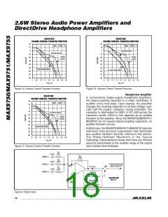
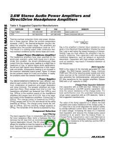
Figure 9. Bridge-Tied Load Configuration
Figure 10. Total Harmonic Distortion Plus Noise vs. Output Power
with Inputs In/Out of Phase (Headphone Mode)
Power Dissipation and Heat Sinking
Under normal operating conditions, the MAX9750/
MAX9751/MAX9755 can dissipate a significant amount
of power. The maximum power dissipation for each
package is given in the Absolute Maximum Ratings
under Continuous Power Dissipation, or can be calcu-
lated by the following equation:
Applications Information
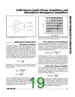
BTL Speaker Amplifiers
The MAX9750/MAX9751/MAX9755 feature speaker
amplifiers designed to drive a load differentially, a con-
figuration referred to as bridge-tied load (BTL). The BTL
configuration (Figure 9) offers advantages over the sin-
gle-ended configuration, where one side of the load is
connected to ground. Driving the load differentially
doubles the output voltage compared to a single-
ended amplifier under similar conditions. Thus, the
device’s differential gain is twice the closed-loop gain
of the input amplifier. The effective gain is given by:
T
− T
A
J(MAX)
P
=
DISSPKG(MAX)
θ
JA
where T
is +150°C, T is the ambient tempera-
A
J(MAX)
ture, and θ is the reciprocal of the derating factor in
JA
°C/W as specified in the Absolute Maximum Ratings
section. For example, θ of the thin QFN package is
JA
R
F
A
= 2×
+42°C/W. For optimum power dissipation, the exposed
paddle of the package should be connected to the
ground plane (see the Layout and Grounding section).
VD
R
IN
Substituting 2 X V
into the following equation
OUT(P-P)
yields four times the output power due to double the
output voltage:
Output Power (Speaker Amplifier)
The increase in power delivered by the BTL configura-
tion directly results in an increase in internal power dis-
sipation over the single-ended configuration. The
V
OUT(P−P)
V
=
=
RMS
maximum power dissipation for a given V
given by the following equation:
and load is
DD
2 2
2
V
RMS
P
2
OUT
2V
DD
R
P
=
L
DISS(MAX)
2
π R
Since the differential outputs are biased at midsupply,
there is no net DC voltage across the load. This elimi-
nates the need for DC-blocking capacitors required for
single-ended amplifiers. These capacitors can be large
and expensive, can consume board space, and can
degrade low-frequency performance.
If the power dissipation for a given application exceeds
the maximum allowed for a given package, either reduce
DD
temperature, or add heatsinking to the device. Large
output, supply, and ground PC board traces improve the
maximum power dissipation in the package.
V
, increase load impedance, decrease the ambient
______________________________________________________________________________________ 19

 MAXIM [ MAXIM INTEGRATED PRODUCTS ]