Low-Cost, Ultra-Small, Single/Dual/Quad
Single-Supply Comparators
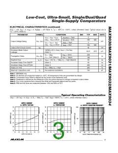
ELECTRICAL CHARACTERISTICS (continued)
(V
= +5V, V
= +25°C.) (Note 2)
= 0, V
= 0, V
= +5V (Note 1), T = -40°C to +125°C, unless otherwise noted. Typical values are at
SHDN A
DD
SS
CM
T
A
PARAMETER
SYMBOL
CONDITIONS
MIN
TYP
2
MAX
400
UNITS
I
I
I
I
= 10µA
= 4mA
SOURCE
SOURCE
V
(V
= V
IN+
- V
,
OH
DD
OUT
- V ) ≥ 20mV
IN-
165
2
Output Voltage-Swing
V
, V
OL OH
mV
= 10µA
SINK
SINK
V
= V
- V
SS
,
OL
OUT
(V - V ) ≥ 20mV
IN-
IN+
= 4mA
165
45
400
Output Short-Circuit Current
I
mA
SC
Shutdown Mode Output
Leakage
V
≤ (0.3 × V ), V
= 0 to V
OUT DD
SHDN
DD
0.01
3.5
µA
(Note 1)
V
V
= 10mV
228
188
20
R = 10kΩ,
C = 15pF (Note 5)
L
OD
OD
L
Propagation Delay
t
, t
ns
PD+ PD-
= 100mV
Rise/Fall-Time
t , t
V
= +5V, R = 10kΩ, C = 15pF (Note 6)
ns
ns
ns
ns
pF
R
F
DD
L
L
Shutdown Delay Time ON/OFF
Shutdown Delay Time OFF/ON
Power-On Time
(Note 1)
(Note 1)
40
400
200
150
R = 10kΩ, C = 15pF
L
L
Maximum Capacitive Load
C
No sustained oscillations
L
Note 1: MAX9030 only.
Note 2: All devices are production tested at +25°C. All temperature limits are guaranteed by design.
Note 3: Comparator Input Offset is defined as the center of the hysteresis zone.
Note 4: Hysteresis is defined as the difference of the trip points required to change comparator output states.
Note 5: V is the overdrive that is beyond the offset and hysteresis-determined trip points.
OD
Note 6: Rise and fall times are measured between 10% and 90% at OUT.
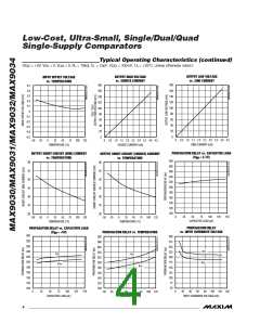
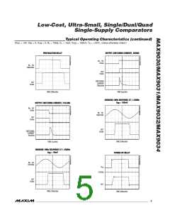
Typical Operating Characteristics
(V
= +5V, V = 0, V
= 0, R = 10kΩ, C = 15pF, V = 100mV, T = +25°C, unless otherwise noted.)
DD
SS
CM
L
L
A
OD
SUPPLY CURRENT
vs. SUPPLY VOLTAGE
SUPPLY CURRENT
vs. TEMPERATURE
SUPPLY CURRENT
vs. OUTPUT TRANSITION FREQUENCY
40
38
36
34
32
30
28
38
37
36
35
34
33
32
1000
100
10
2.5
3.0
3.5
4.0
4.5
5.0
5.5
-50 -25
0
25
50
75 100 125
100
10k
100k
1M
10
1k
SUPPLY VOLTAGE (V)
TEMPERATURE (°C)
OUTPUT TRANSITION FREQUENCY (Hz)
_______________________________________________________________________________________
3

 MAXIM [ MAXIM INTEGRATED PRODUCTS ]