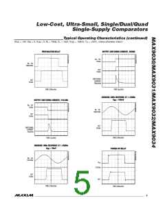
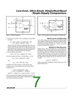
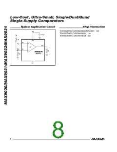
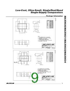
Low-Cost, Ultra-Small, Single/Dual/Quad
Single-Supply Comparators
ABSOLUTE MAXIMUM RATINGS
Supply Voltage (V
to V ) ....................................-0.3V to +6V
8-Pin SOT23 (derate 9.1mW/°C above +70°C).............727mW
8-Pin µMAX (derate 4.5mW/°C above +70°C)..............362mW
8-Pin SO (derate 5.88mW/°C above +70°C).................471mW
14-Pin TSSOP (derate 9.1mW/°C above +70°C) ..........727mW
14-Pin SO (derate 8.33mW/°C above +70°C)...............667mW
Operating Temperature Range
DD
SS
Voltage Inputs (IN+, IN- to V ). ................-0.3V to (V
+ 0.3V)
SS
DD
Differential Input Voltage (IN+ to IN-) .................................+6.6V
Output Short-Circuit
Duration ...............................................2s to Either V
or V
DD
SS
Current into Any Pin ............................................................20mA
Continuous Power Dissipation (T = +70°C) ...............................
Automotive Application...................................-40°C to +125°C
Junction Temperature......................................................+150°C
Storage Temperature Range.............................-65°C to +150°C
Lead Temperature (soldering, 10s) ................................ +300°C
A
5-Pin SC70 (derate 3.1mW/°C above +70°C)...............247mW
5-Pin SOT23 (derate 7.1mW/°C above +70°C).............571mW
6-Pin SC70 (derate 3.1mW/°C above +70°C)...............245mW
6-Pin SOT23 (derate 8.7mW/°C above +70°C).............696mW
Stresses beyond those listed under “Absolute Maximum Ratings” may cause permanent damage to the device. These are stress ratings only, and functional
operation of the device at these or any other conditions beyond those indicated in the operational sections of the specifications is not implied. Exposure to
absolute maximum rating conditions for extended periods may affect device reliability.
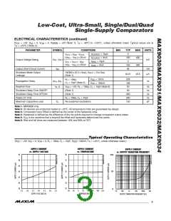
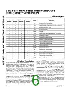
ELECTRICAL CHARACTERISTICS
(V
= +5V, V
= +25°C.) (Note 2)
= 0, V
= 0, V
= +5V (Note 1), T = -40°C to +125°C, unless otherwise noted. Typical values are at
SHDN A
DD
SS
CM
T
A
PARAMETER
SYMBOL
CONDITIONS
Guaranteed by PSRR test
MIN
TYP
MAX
5.5
55
UNITS
V
2.5
Operating Voltage Range
V
DD
DD
Supply Current per Comparator
Supply Current in Shutdown
Shutdown Input Bias Current
Shutdown Logic High
I
35
0.05
0.1
µA
µA
µA
V
V
V
= 0 (Note 1)
1
S HDN
S HDN
= 0 to V
(Note 1)
2.5
DD
0.7 × V
(Note 1)
(Note 1)
(Note 3)
DD
0.3 × V
Shutdown Logic Low
V
DD
Input Offset Voltage
V
1
1
5
mV
OS
Input Offset Voltage
Temperature Coefficient
TCV
µV/°C
OS
Hysteresis
(Note 4)
4
8
2
mV
nA
nA
V
Input Bias Current
I
80
60
BIAS
Input Offset Current
Common-Mode Voltage Range
Common-Mode Rejection Ratio
I
OS
V
Guaranteed by CMRR test
V
V
- 1.1
CM
SS
DD
CMRR
PSRR
V
SS
≤ V ≤ (V - 1.1V), V = +5.5V
72
72
100
100
dB
CM
DD
DD
Power-Supply Rejection Ratio
V
= +2.5V to +5.5V
dB
DD
2
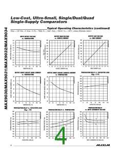
_______________________________________________________________________________________

 MAXIM [ MAXIM INTEGRATED PRODUCTS ]