Low-Cost, Ultra-Small, Single/Dual/Quad
Single-Supply Comparators
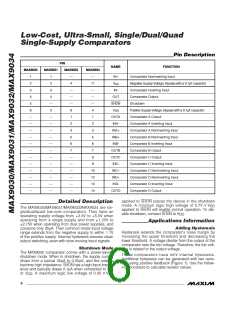
V
DD
R1
V
DD
V
DD
V
DD
R2
IN+
IN-
IN+
IN-
V
IN
V
REF
OUT
OUT
10kΩ
V
MAX9031
IN
0.1µF
V
SS
MAX9031
V
SS
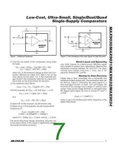
Figure 1. Additional Hysteresis
Figure 2. Time Averaging of the Input Signal for Data Recovery
1) Find the trip points of the comparator using these
formulas:
Board Layout and Bypassing
Use 100nF bypass as a starting point. Minimize signal
trace lengths to reduce stray capacitance. Minimize the
capacitive coupling between IN- and OUT. For slow-
moving input signals (rise-time > 1ms), use a 1nF
capacitor between IN+ and IN-.
V
TH
= V
+[((V
REF
- V
)R2) / (R1 + R2)
REF
REF
= V
DD
V
(1 - (R2 / (R1 + R2))]
TL
where V is the threshold voltage at which the com-
TH
parator switches its output from high to low as V
IN
Biasing for Data Recovery
rises above the trip point. V is the threshold volt-
TL
Digital data is often embedded into a bandwidth and
amplitude-limited analog path. Recovering the data can
be difficult. Figure 2 compares the input signal to a
time-averaged version of itself. This self-biases the
threshold to the average input voltage for optimal noise
margin. Even severe phase distortion is eliminated from
the digital output signal. Be sure to choose R1 and C1
so that:
age at which the comparator switches its output from
low to high as V drops below the trip point.
IN
2) The hysteresis band will be:
V
HYS
= V - V = V (R2 / (R1 + R2))
TH TL DD
3) In this example, let V
= +5V and V
= +2.5V.
DD
REF
V
TH
= 2.5V + 2.5(R2 / (R1 + R2))V
ƒ
CAR
>> 1 / (2πR1C1)
and
where ƒ
is the fundamental carrier frequency of the
CAR
V
= 2.5[1 - (R2 / (R1 + R2))]
TL
digital data stream.
4) Select R2. In this example, we will choose 1kΩ.
5) Select V . In this example, we will choose 50mV.
HYS
6) Solve for R1.
V
HYS
= V (R2 / (R1 + R2))
DD
0.050V = 5(1000Ω/(R1 + 1000Ω)) V
where R1 ≈ 100kΩ, V = 2.525V, and V = 2.475V.
TH
TL
The above-described design procedure assumes rail-
to-rail output swing. If the output is significantly loaded,
the results should be corrected.
_______________________________________________________________________________________
7

 MAXIM [ MAXIM INTEGRATED PRODUCTS ]