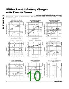
SMBus Level 2 Battery Charger
with Remote Sense
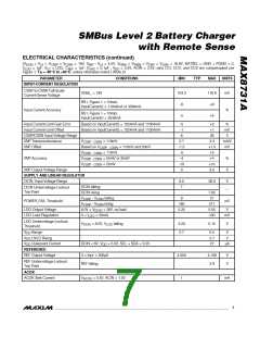
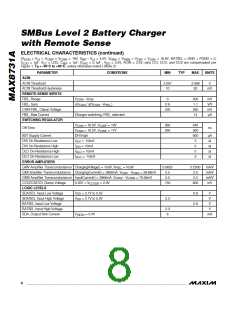
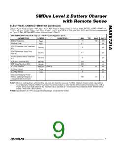
ELECTRICAL CHARACTERISTICS
(V
= V = V
= V
= 19V, V
- V = 4.5V, V
= V
= V
= V
= 16.8V, BATSEL = GND = PGND = 0,
CSIN
DCIN
LDO
LX
CSSP
CSSN
REF
BST
DAC
LX
FBSA
FBSB
CSIP
C
= 1µF, V
= LDO, C
= 1µF, C
= 0.1µF , V
= 3.3V, ACIN = 2.5V; pins CCI, CCV, and CCS are compensated per
CC
DD
Figure 1; T = -40°C to +85°C, unless otherwise noted.) (Note 2)
A
PARAMETER
CONDITIONS
MIN
TYP
MAX
UNITS
CHARGE-VOLTAGE REGULATION
16.632
-1
16.968
+1
V
%
V
ChargingVoltage() = 0x41A0
ChargingVoltage() = 0x3130
ChargingVoltage() = 0x20D0
ChargingVoltage() = 0x1060
12.466
-1
12.717
+1
%
V
Battery Full-Charge Voltage and
Accuracy
8.316
-1
8.484
+1
%
V
4.129
-1.5
4.255
+1.5
%
CHARGE-CURRENT REGULATION
CSIP-to-CSIN Full-Scale Current-
Sense Voltage
78.22
83.05
mV
7.822
-3
8.305
+3
A
%
A
RS2, Figure 1 = 10mΩ;
ChargingCurrent()= 0x1f80
3.809
-4
4.126
+4
RS2, Figure 1 = 10mΩ;
ChargingCurrent() = 0x0f80
Charge Current and Accuracy
Charge-Current Gain Error
%
RS2, Figure 1 =10mΩ;
ChargingCurrent() = 0x0080
30
-2
0
400
+2
19
mA
%
Based on ChargeCurrent() = 128mA and 8.064A
FBSA/FBSB/CSIP/CSIN Input-
Voltage Range
V
Adapter present, not charging, I
+ I
+ I + I
,
CSIP
CSIN
LX
FBS
5
1
V
= V = V
= V
= 19V
CSIP
FBS_
LX
CSIN
Battery Quiescent Current
Adapter Quiescent Current
µA
Adapter absent, I
+ I
+ I + I
+ I
+
CSIP
CSIN
LX
FBSA
= V = 19V,
CSIP
FBSB
I
+ I
, V
= V = V
CSSP
CSSN FBS_
LX
CSIN
V
= 0V
DCIN
V
= 26V, V
= 16.8V, not charging
Charging
500
1
µA
mA
µA
Adapter
Battery
V
V
= 19V,
= 16.8V
I
I
I
+
+
Adapter
Battery
DCIN
CSSP
CSSN
Not charging
Charging
500
1
mA
µA
V
V
= 8V,
= 4V
Adapter
Battery
Not charging
500
6
_______________________________________________________________________________________

 MAXIM [ MAXIM INTEGRATED PRODUCTS ]