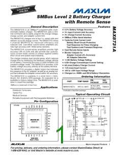
SMBus Level 2 Battery Charger
with Remote Sense
ABSOLUTE MAXIMUM RATINGS
DCIN, CSSN, CSIN, FBSA, FBSB to GND..............-0.3V to +28V
CSSP to CSSN, CSIP to CSIN, PGND to GND ......-0.3V to +0.3V
BST to GND............................................................-0.3V to +32V
BST to LX..................................................................-0.3V to +6V
V
, SCL, SDA, BATSEL, ACIN, ACOK, V
LDO to PGND......................................................-0.3V to +6V
to GND,
DD
CC
Continuous Power Dissipation (T = +70°C)
A
28-Pin Thin QFN
DHI to LX.................................................-0.3V to +(V
+ 0.3)V
(derate 20.8mW/°C above +70°C)........................1666.7 mW
Operating Temperature Range ...........................-40°C to +85°C
Junction Temperature......................................................+150°C
Storage Temperature Range.............................-60°C to +150°C
Lead Temperature (soldering, 10s) .................................+300°C
BST
DLO to PGND..........................................-0.3V to +(LDO + 0.3)V
LX to GND .................................................................-6V to +28V
CCI, CCS, CCV, DAC, REF,
IINP to GND...........................................-0.3V to (V
+ 0.3)V
VCC
Stresses beyond those listed under “Absolute Maximum Ratings” may cause permanent damage to the device. These are stress ratings only, and functional
operation of the device at these or any other conditions beyond those indicated in the operational sections of the specifications is not implied. Exposure to
absolute maximum rating conditions for extended periods may affect device reliability.
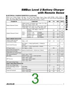
ELECTRICAL CHARACTERISTICS
(V
= V = V
= V
= 19V, V
- V = 4.5V, V
= V
= V
= V
= 16.8V, BATSEL = GND = PGND = 0,
CSIN
DCIN
LX
CSSP
CSSN
BST
LX
FBSA
FBSB
CSIP
C
LDO
= 1µF, V
= LDO, C
= 1µF, C
= 0.1µF, V
= 3.3V, ACIN = 2.5V; pins CCI, CCV, and CCS are compensated per
CC
REF
DAC
DD
Figure 1; T = 0°C to +85°C, unless otherwise noted. Typical values are at T = +25°C.)
A
A
PARAMETER
CONDITIONS
MIN
TYP
MAX
UNITS
CHARGE-VOLTAGE REGULATION
16.716
-0.5
16.8
16.884
+0.5
V
%
V
ChargingVoltage() = 0x41A0
12.491 12.592 12.693
ChargingVoltage() = 0x3130
ChargingVoltage() = 0x20D0
ChargingVoltage() = 0x1060
-0.8
8.333
-0.8
+0.8
8.467
+0.8
%
V
Battery Full-Charge Voltage and
Accuracy
8.4
%
V
4.150
-1.0
4.192
4.234
+1.0
%
Battery Undervoltage-Lockout
Trip Point for Trickle Charge
2.5
V
CHARGE-CURRENT REGULATION
CSIP-to-CSIN Full-Scale Current-
Sense Voltage
78.22
80.64
8.064
83.06
mV
7.822
-3
8.306
+3
A
%
A
RS2, Figure 1 = 10mΩ;
ChargingCurrent() = 0x1f80
3.809
-4
3.968
4.126
+4
RS2, Figure 1 = 10mΩ;
ChargingCurrent() = 0x0f80
Charge Current and Accuracy
Charge-Current Gain Error
%
RS2, Figure 1 = 10mΩ;
ChargingCurrent() = 0x0080 (128mA)
64
-2
0
400
+2
19
mA
%
Based on ChargeCurrent() = 128mA and 8.064A
FBSA/FBSB/CSIP/CSIN
Input Voltage Range
V
2
_______________________________________________________________________________________

 MAXIM [ MAXIM INTEGRATED PRODUCTS ]