SMBus Level 2 Battery Charger
with Remote Sense
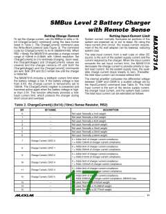
Pin Description
PIN
NAME
GND
ACIN
REF
FUNCTION
1, 12
Analog Ground. Connect directly to the paddle.
2
3
4
5
6
7
AC Adapter Detect Input. ACIN is the input to an uncommitted comparator.
4.096V Voltage Reference. Bypass REF with a 1µF capacitor to GND.
Input Current Regulation Loop-Compensation Point. Connect 0.01µF from CCS to GND.
Output Current Regulation Loop-Compensation Point. Connect 0.01µF from CCI to GND.
Voltage Regulation Loop-Compensation Point. Connect 10kΩ in series with 0.01µF to GND.
DAC Voltage Output. Bypass with 0.1µF from DAC to GND.
CCS
CCI
CCV
DAC
Input Current Monitor Output. IINP sources the current proportional to the current sensed across
CSSP and CSSN. The transconductance from (CSSP - CSSN) to IINP is 3mA/V.
8
IINP
9
SDA
SCL
SMBus Data I/O. Open-drain output. Connect an external pullup resistor according to SMBus specifications.
SMBus Clock Input. Connect an external pullup resistor according to SMBus specifications.
Logic Circuitry Supply-Voltage Input. Bypass with a 0.1µF capacitor to GND.
10
11
V
DD
AC Detect Output. This open-drain output is high impedance when ACIN is greater than REF/2. The
ACOK output remains low when the MAX8731A is powered down. Connect a 10kΩ pullup resistor from
13
ACOK
V
to ACOK.
CC
Battery Voltage Select Input. Drive BATSEL high to select battery B, or drive BATSEL low to select battery A.
Any change of BATSEL immediately stops charging. Charging begins again in approximately 10ms.
14
15
16
BATSEL
FBSA
Remote-Sense Input for the Output Voltage of Battery A. Connect a 100Ω resistor from FBSA to the
battery connector, and a 10nF capacitor from FBSA to PGND.
Remote-Sense Input for the Output Voltage of Battery B. Connect a 100Ω resistor from FBSB to the
battery connector, and a 10nF capacitor from FBSB to PGND.
FBSB
17
18
19
CSIN
CSIP
Charge Current-Sense Negative Input
Charge Current-Sense Positive Input. Connect a 10mΩ current-sense resistor between CSIP and CSIN.
PGND
Power Ground
Low-Side Power MOSFET Driver Output. Connect to low-side n-channel MOSFET. DLO drives
between LDO and PGND.
20
DLO
LDO
Linear-Regulator Output. LDO is the output of the 5.4V linear regulator supplied from DCIN. LDO also
directly supplies the DLO driver and the BST charge pump. Bypass with a 1µF ceramic capacitor
from LDO to PGND.
21
22
23
DCIN
LX
Charger Bias Supply Input. Bypass DCIN with a 0.1µF capacitor to PGND.
High-Side Power MOSFET Driver Source Connection. Connect to the source of the high-side n-channel
MOSFET.
24
25
26
27
28
—
DHI
BST
High-Side Power MOSFET Driver Output. Connect to the high-side n-channel MOSFET gate.
High-Side Power MOSFET Driver Power-Supply Connection. Connect a 0.1µF capacitor from BST to LX.
Device Power-Supply Input. Connect to LDO through an RC filter as shown in Figure 1.
Input Current-Sense Negative Input
V
CC
CSSN
CSSP
BP
Input Current-Sense Positive Input. Connect a 10mΩ current-sense resistor between CSSP and CSSN.
Backside Paddle. Connect the backside paddle to analog ground.
______________________________________________________________________________________ 13

 MAXIM [ MAXIM INTEGRATED PRODUCTS ]