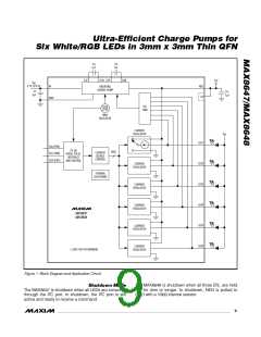
Ultra-Efficient Charge Pumps for
Six White/RGB LEDs in 3mm x 3mm Thin QFN
ABSOLUTE MAXIMUM RATINGS
V
DD
V
DD
, IN, SCL, SDA, ENA, ENB, ENC to GND........-0.3V to +6.0V
, IN, SCL, SDA, ENA, ENB, ENC to NEG........-0.3V to +6.0V
Continuous Power Dissipation (T = +70°C)
A
16-Pin Thin QFN 3mm x 3mm (derate 20.8mW/°C
NEG to GND.............................................................-6V to +0.3V
C2N to GND .............................................................-6V to +0.3V
above +70°C).............................................................1667mW
Junction Temperature......................................................+150°C
Storage Temperature Range.............................-65°C to +150°C
Lead Temperature (soldering, 10s) .................................+300°C
C1P, C2P to GND .......................................-0.3V to (V + 0.3V)
IN
C2P to C1N..................................................-0.3V to (V + 0.3V)
IN
LED_, C1N, C2N to NEG .............................-0.3V to (V + 0.3V)
IN
Stresses beyond those listed under “Absolute Maximum Ratings” may cause permanent damage to the device. These are stress ratings only, and functional
operation of the device at these or any other conditions beyond those indicated in the operational sections of the specifications is not implied. Exposure to
absolute maximum rating conditions for extended periods may affect device reliability.
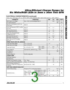
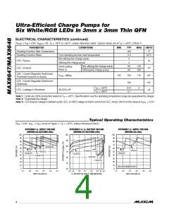
ELECTRICAL CHARACTERISTICS
(V
= V = 3.6V, V
= 0V, T = -40°C to +85°C, unless otherwise noted. Typical values are at T = +25°C.) (Note 1)
GND A A
VDD
IN
PARAMETER
IN Operating Voltage
Operating Voltage
CONDITIONS
MIN
TYP
MAX
5.5
UNITS
7/MAX648
2.7
1.7
V
V
V
5.5
DD
Undervoltage-Lockout (UVLO)
Threshold
V
rising
2.35
2.45
2.55
V
IN
Undervoltage-Lockout Hysteresis
100
0.4
0.4
0.1
0.1
mV
µA
T
T
= +25°C
= +85°C
2.5
1.0
A
IN Shutdown Supply Current
(All Outputs Off)
V
V
= V
= V
(MAX8647),
DD
SCL
SDA
_ = 0V (MAX8648)
EN
A
T
T
= +25°C
= +85°C
A
V
Shutdown Supply Current
µA
µA
DD
A
Charge pump inactive, two LEDs enabled at 0.1mA
setting
70
1.6
0.1
0.1
100
1.0
IN Operating Supply Current
Charge pump active, 1MHz switching, all LEDs
enabled at 0.1mA setting
mA
Charge pump inactive, two LEDs enabled at 0.1mA
setting, T = +25°C
A
V
Operating Supply Current
µA
DD
Charge pump active, 1MHz switching, all LEDs
enabled at 0.1mA setting, T = +85°C
A
Thermal-Shutdown Threshold
Thermal-Shutdown Hysteresis
+160
20
°C
°C
2
I C INTERFACE (MAX8647)
0.7 x
Logic-Input High Voltage (SDA, SCL)
Logic-Input Low Voltage (SDA, SCL)
V
= 1.7V to 5.5V, hysteresis = 0.2 x V
= 1.7V to 5.5V, hysteresis = 0.2 x V
(typ)
(typ)
V
DD
DD
DD
V
DD
0.3 x
V
V
V
V
DD
V
DD
Filtered Pulse Width (t
)
= 2.7V to 5.5V, V = 1.7V to 5.5V (Note 2)
DD
50
+1
ns
µA
SP
IN
IL
T
A
T
A
= +25°C
= +85°C
-1
0.01
0.1
Logic-Input Current (SDA, SCL)
= 0V or V = 5.5V
IH
2
_______________________________________________________________________________________

 MAXIM [ MAXIM INTEGRATED PRODUCTS ]