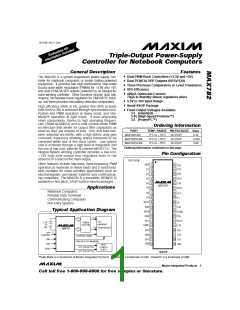
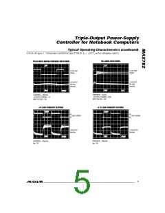
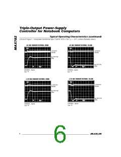
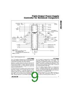
Trip le -Ou t p u t P o w e r-S u p p ly
Co n t ro lle r fo r No t e b o o k Co m p u t e rs
ABSOLUTE MAXIMUM RATINGS
V+ to GND.................................................................-0.3V, +36V
PGND to GND........................................................................±2V
VL to GND ...................................................................-0.3V, +7V
BST3, BST5 to GND ..................................................-0.3V, +36V
LX3 to BST3.................................................................-7V, +0.3V
LX5 to BST5.................................................................-7V, +0.3V
Inputs/Outputs to GND
DH3 to LX3 ..................................................-0.3V, (BST3 + 0.3V)
DH5 to LX5 ..................................................-0.3V, (BST5 + 0.3V)
REF, VL, VPP Short to GND........................................Momentary
REF Current.........................................................................20mA
VL Current...........................................................................50mA
VPPA, VPPB Current .........................................................100mA
Continuous Power Dissipation (TA = +70°C)
MAX782
(D1-D3, ON5, REF, SYNC, DA1, DA0, DB1, DB0, ON5,
SSOP (derate 11.76mW/°C above +70°C) ...................941mW
Operating Temperature Ranges:
MAX782CBX/MAX782__CBX...............................0°C to +70°C
MAX782EBX/MAX782__EBX ............................-40°C to +85°C
Storage Temperature Range .............................-65°C to +160°C
Lead Temperature (soldering, 10sec) .............................+300°C
SS5, CS5, FB5, CS3, FB3, SS3, ON3) ..........-0.3V, (VL + 0.3V)
VDD to GND.................................................................-0.3V, 20V
VPPA, VPPB to GND.....................................-0.3V, (VDD + 0.3V)
VH to GND ...................................................................-0.3V, 20V
Q1-Q3 to GND.................................................-0.3V, (VH + 0.3V)
DL3, DL5 to PGND...........................................-0.3V, (VL + 0.3V)
Stresses beyond those listed under “Absolute Maximum Ratings‘” may cause permanent damage to the device. These are stress ratings only, and functional
operation of the device at these or any other conditions beyond those indicated in the operational sections of the specifications is not implied. Exposure to
absolute maximum rating conditions for extended periods may affect device reliability.
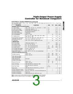
ELECTRICAL CHARACTERISTICS
(V+ = 15V, GND = PGND = 0V, IVL = IREF = 0mA, ON3 = ON5 = 5V, other digital input levels are 0V or +5V, TA = TMIN to TMAX
,
unless otherwise noted.)
PARAMETER
CONDITIONS
MIN
TYP
MAX UNITS
+3.3V AND 5V STEP-DOWN CONTROLLERS
Input Supply Range
5.5
30
V
V
0mV < (CS5-FB5) < 70mV, 6V < V+ < 30V
(includes load and line regulation)
FB5 Output Voltage
4.80
5.08
5.20
MAX782
3.17
3.32
3.46
3.35
3.50
3.65
2
3.46
3.60
3.75
V
V
0mV < (CS3-FB3) < 70mV, 6V < V+ < 30V
(includes load and line regulation)
FB3 Output Voltage
MAX782R
MAX782S
V
Load Regulation
Line Regulation
Either controller (CS_ - FB_ = 0mV to 70mV)
Either controller (V+ = 6V to 30V)
CS3-FB3 or CS5-FB5
%
0.03
100
-100
4.0
%/V
80
-50
2.5
2
120
-160
6.5
Current-Limit Voltage
mV
CS5-FB5 (VDD < 13V, flyback mode)
SS3/SS5 Source Current
SS3/SS5 Fault Sink Current
15V FLYBACK CONTROLLER
VDD Regulation Setpoint
VDD Shunt Setpoint
µA
mA
Falling edge, hysteresis = 1%
Rising edge, hysteresis = 1%
VDD = 20V
13
18
2
14
20
V
V
VDD Shunt Current
3
mA
VDD = 18V, ON3 = ON5 = 5V,
VPPA/B programmed to 12V with no external load
Quiescent VDD Current
140
300
30
µA
µA
VDD = 18V, ON3 = ON5 = 5V,
VPPA/B programmed to Hi-Z or 0V
VDD Off Current
15
PCMCIA REGULATORS (Note 1)
Program to 12V, 13V < VDD < 19V, 0mA < I < 60mA
11.6
4.85
-0.3
12.1
5.05
12.5
5.20
0.3
L
VPPA/VPPB Output Voltage
VPPA/VPPB Off Input Current
Program to 5V, 13V < VDD < 19V, 0mA < I < 60mA
V
L
Program to 0V, 13V < VDD < 19V, -0.3mA < I < 0.3mA
L
Program to Hi-Z, VDD = 19V, 0V < VPP < 12V
35
µA
2
_______________________________________________________________________________________

 MAXIM [ MAXIM INTEGRATED PRODUCTS ]