±1 5 k V ES D-P ro t e c t e d , S in g le /Du a l/Oc t a l,
CMOS S w it c h De b o u n c e rs
7/MAX618
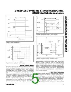
t
DP
EN
t
EN
IN1
1
V
1
V
/2 CC
/2 CC
t
PE
t
OUT1–OUT8
PD
OUT NORMALLY
LOW
OUT1
1
V
/2 CC
V
OL
+ 0.5V
- 0.5V
t
PE
OUT NORMALLY
HIGH
1
V
V
/2 CC
OH
OUT1–OUT8
CH
IN2
t
PD
t
PC
1
V
/2 CC
OUT2
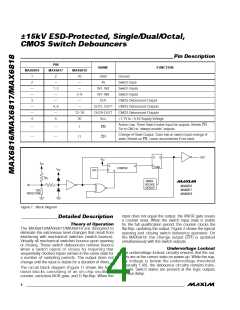
Figure 4. MAX6818 µP-Interface Timing Diagram
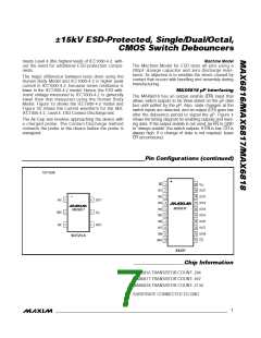
CH
+V
CC
MAX6818 ONLY
+V
CC
0.1µF
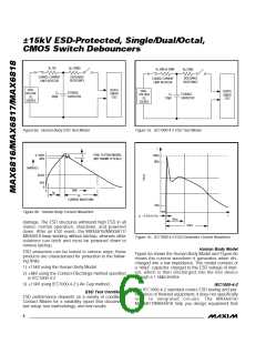
Figure 2. Input Characteristics
SW1
EN
CH
I/O
IN1
IN8
µP
IRQ
20V
MAX6818
IN
0
(20V/div)
-20V
OUT1
OUT8
D0
D7
SW8
4V
OUT
(2V/div)
0
Figure 5. MAX6818 Typical µP Interfacing Circuit
20ms/div
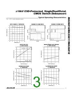
approximately 0.5mA (up to 4mA for eight inputs) from
the V supply. Driving an input to +25V will cause
CC
Figure 3. Switch Input ±25V Fault Tolerance
approximately 0.32mA of current (up to 2.6mA for eight
inputs) to flow back into the V supply. If the total sys-
CC
Ro b u s t S w it c h In p u t s
tem V supply current is less than the current flowing
CC
The switch inputs on the MAX6816/MAX6817/MAX6818
have overvoltage clamping diodes to protect against
d a ma g ing fa ult c ond itions . Switc h inp ut volta g e s
can safely swing ±25V to ground (Figure 3). Proprietary
ESD-p rote c tion s truc ture s p rote c t a g a ins t hig h
ESD encountered in harsh industrial environments,
me mb ra ne ke yp a d s , a nd p orta b le a p p lic a tions .
The y a re d e s ig ne d to withs ta nd ± 15kV p e r the
IEC1000-4-2 Air Gap Discharge Test and ±8kV per the
IEC1000-4-2 Contact Discharge Test.
back into the V
supply, V
will rise above normal
CC
CC
levels. In some low-current systems, a zener diode on
may be required.
V
CC
±1 5 k V ES D P ro t e c t io n
As with all Maxim devices, ESD-protection structures
are incorporated on all pins to protect against electro-
static discharges encountered during handling and
a s s e mb ly. The MAX6816/MAX6817/MAX6818 ha ve
extra protection against static electricity. Maxim's engi-
neers have developed state-of-the-art structures to pro-
tect against ESD of ±15kV at the switch inputs without
Since there are 63kΩ (typical) pull-up resistors con-
nected to each input, driving an input to -25V will draw
_______________________________________________________________________________________
5

 MAXIM [ MAXIM INTEGRATED PRODUCTS ]