±1 5 k V ES D-P ro t e c t e d , S in g le /Du a l/Oc t a l,
CMOS S w it c h De b o u n c e rs
ABSOLUTE MAXIMUM RATINGS
Voltage (with respect to GND)
Continuous Power Dissipation (T = +70°C)
A
V
.......................................................................-0.3V to +6V
4-Pin SOT143 (derate 4.0mW/°C above +70°C)..........320mW
6-Pin SOT23 (derate 8.7mW/°C above +70°C)............691mW
20-Pin SSOP (derate 8.0mW/°C above +70°C) ...........640mW
Operating Temperature Range ...........................-40°C to +85°C
Storage Temperature Range .............................-65°C to +160°C
Lead Temperature (soldering, 10sec) .............................+300°C
CC
IN_ (Switch Inputs) ..............................................-30V to +30V
EN.........................................................................-0.3V to +6V
OUT_, CH ...............................................-0.3V to (V + 0.3V)
OUT Short-Circuit Duration
CC
(One or Two Outputs to GND)....................................Continuous
Stresses beyond those listed under “Absolute Maximum Ratings” may cause permanent damage to the device. These are stress ratings only, and functional
operation of the device at these or any other conditions beyond those indicated in the operational sections of the specifications is not implied. Exposure to
absolute maximum rating conditions for extended periods may affect device reliability.
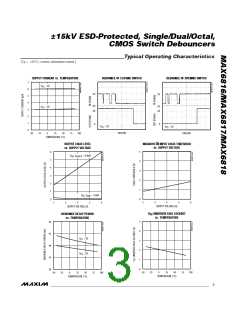
ELECTRICAL CHARACTERISTICS
(V = +2.7V to +5.5V, T = -40°C to +85°C, unless otherwise noted. Typical values are at V = +5V, T = +25°C.) (Note 1)
CC
A
CC
A
PARAMETER
SYMBOL
CONDITIONS
MIN
TYP
MAX UNITS
Operating Voltage Range
Supply Current
V
2.7
5.5
20
V
CC
I
CC
V
CC
= 5V, I
= 0, IN_ = V
CC
6
µA
OUT
MAX6818
MAX6816/MAX6817
20
20
40
50
60
Debounce Duration
t
ms
V
DP
80
V
0.8
IL
Input Threshold
V
= 5V
2.4
2.0
CC
V
IH
V
V
CC
= 2.7V
Input Hysteresis
300
63
mV
kΩ
mA
V
Input Pull-Up Resistance
IN Input Current
32
100
±1
I
V = ±15V
IN
IN
7/MAX618
Input Voltage Range
Undervoltage-Lockout Threshold
V
-25
25
IN
1.9
2.6
0.4
V
V
OL
I
= 1.6mA
SINK
V
ns
V
OUT_, CH Output Voltage
EN Pulse Width
V
OH
I
= 0.4mA
V
- 1.0
SOURCE
CC
t
200
EN
V
CC
= 5V
0.8
0.8
1.7
1.1
2.4
2.0
±1
EN Threshold
V
CC
= 2.7V
I
µA
ns
EN Input Current
IL
EN Low to Out Active
Propagation Delay
t
R
R
R
= 10kΩ, C = 100pF
100
100
PE
PD
PC
L
L
L
L
EN High to Out Three-State
Propagation Delay
t
t
= 1kΩ, C = 15pF
ns
L
EN Low to CH Out High
Propagation Delay
= 10kΩ, C = 50pF
100
±10
ns
L
V
OUT
= 0 or V
µA
OUT_ Three-State Leakage Current
CC
ESD CHARACTERISTICS
IEC1000-4-2 Air Discharge
±15
±8
ESD Protection
IN_
IEC1000-4-2 Contact Discharge
Human Body Model
kV
±15
Note 1: MAX6816 and MAX6817 production testing is done at T = +25°C; over-temperature limits are guaranteed by design.
A
2
_______________________________________________________________________________________

 MAXIM [ MAXIM INTEGRATED PRODUCTS ]