±1 5 k V ES D-P ro t e c t e d , S in g le /Du a l/Oc t a l,
CMOS S w it c h De b o u n c e rs
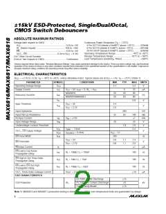
P in De s c rip t io n
PIN
NAME
FUNCTION
MAX6816
MAX6817
MAX6818
1
2
2
—
1, 3
—
—
4, 6
—
5
10
—
GND
IN
Ground
Switch Input
—
—
3
—
IN1, IN2
IN1–IN8
OUT
Switch Inputs
Switch Inputs
CMOS Debounced Output
2–9
—
—
—
4
—
OUT2, OUT1
OUT8–OUT1
CMOS Debounced Outputs
CMOS Debounced Outputs
+2.7V to +5.5V Supply Voltage
12–19
20
V
CC
Active-Low, Three-State Enable Input for outputs. Resets CH.
Tie to GND to “always enable” outputs.
—
—
—
—
1
EN
CH
Change-of-State Output. Goes low on switch input change of
state. Resets on EN. Leave unconnected if not used.
11
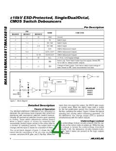
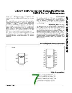
D
Q
OUT
V
CC
V
CC
D
Q
LOAD
COUNTER
V
CC
OSC.
R
7/MAX618
R
PU
UNDER-
VOLTAGE
LOCKOUT
IN
MAX6816
MAX6817
MAX6818
ESD
PROTECTION
Figure 1. Block Diagram
input does not equal the output, the XNOR gate issues
a counter reset. When the switch input state is stable
for the full qualification period, the counter clocks the
flip-flop, updating the output. Figure 2 shows the typical
opening and closing switch debounce operation. On
the MAX6818, the c ha ng e outp ut (CH) is up d a te d
simultaneously with the switch outputs.
_______________De t a ile d De s c rip t io n
Th e o ry o f Op e ra t io n
The MAX6816/MAX6817/MAX6818 a re d e s ig ne d to
eliminate the extraneous level changes that result from
interfacing with mechanical switches (switch bounce).
Virtually all mechanical switches bounce upon opening
or closing. These switch debouncers remove bounce
whe n a s witc h op e ns or c los e s b y re q uiring tha t
sequentially clocked inputs remain in the same state for
a number of sampling periods. The output does not
change until the input is stable for a duration of 40ms.
Un d e rvo lt a g e Lo c k o u t
The undervoltage lockout circuitry ensures that the out-
puts are at the correct state on power-up. While the sup-
p ly volta g e is b e low the und e rvolta g e thre s hold
(typically 1.9V), the debounce circuitry remains trans-
parent. Switch states are present at the logic outputs
without delay.
The circuit block diagram (Figure 1) shows the func-
tiona l b loc ks c ons is ting of a n on-c hip os c illa tor,
counter, exclusive-NOR gate, and D flip-flop. When the
4
_______________________________________________________________________________________

 MAXIM [ MAXIM INTEGRATED PRODUCTS ]