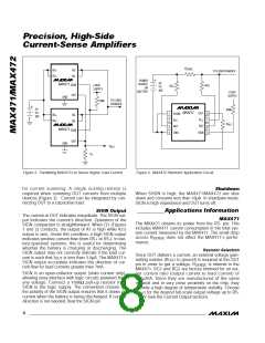
P re c is io n , Hig h -S id e
Cu rre n t -S e n s e Am p lifie rs
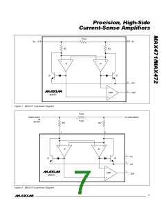
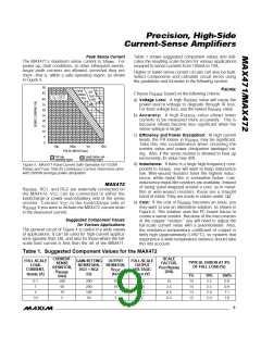
In Figure 6, assume the load current to be measured is
10A and that you have determined a 0.3 inch wide, 2
ounce copper to be appropriate. The resistivity of 0.1
inch wide, 2 ounce copper is 30mΩ/ft (see Note 4). For
TO LOAD/CHARGER
0.3" COPPER
R
SENSE
0.3" COPPER
3V
0.1" COPPER
10A you may want R
= 5mΩ for a 50mV drop at
SENSE
full scale. This resistor will require about 2 inches of 0.1
inch wide copper trace.
POWER
SOURCE
OR
RG1
RG2
TO
36V
BATTERY
RG1 and RG2
Once R
is chosen, RG1 and RG2 can be chosen
SENSE
to define the current-gain ratio (R
/RG). Choose
SENSE
RG = RG1 = RG2 based on the following criteria:
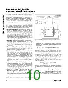
MAX472
a) 1Ω Input Resistance. The minimum RG value is lim-
ited by the 1Ω input resistance, and also by the out-
put current limitation (see below). As RG is reduced,
the input resistance becomes a larger portion of the
total gain-setting resistance. With RG = 50Ω, the
input resistance produces a 2% difference between
the expected and actual current-gain ratio. This is a
gain error that does not affect linearity and can be
OUT
1
2
3
4
8
7
6
5
SHDN
N.C.
V
CC
1.5k
1k
RG2
RG1
1/MAX472
SIGN
GND
removed by adjusting RG or R
.
OUT
Figure 6. MAX472 Connections Showing Use of PC Board
Trace
b) Efficiency. As RG is reduced, I
gets larger for a
OUT
given load current. Power dissipated in R
is not
OUT
going to the load, and therefore reduces overall effi-
ciency. This is significant only when the sense cur-
rent is small.
make sure RG is small enough that I and I
not add any appreciable errors. The full-scale error
is given by:
do
B
OS
c) Maximum Output Current Limitation. I
is limit-
OUT
(RG1 - RG2) x I + I x RG
B
OS
x R
SENSE
% Error =
x 100
ed to 1.5mA, requiring RG ≥ V
/ 1.5mA. For
SENSE
I
FS
V
SENSE
= 60mV, RG must be ≥ 40Ω.
where RG1 and RG2 are the gain resistors, I is the
B
d) Headroom. The MAX472 requires a minimum of
bias current, I is the bias-current mismatch, I is the
OS
FS
1.5V between the lower of the voltage at RG1 or
full-scale current, and R
is the sense resistor.
SENSE
RG2 (V
) and V . As RG becomes larger, the
OUT
RG_
voltage drop across RG also becomes larger for a
given I . This voltage drop further limits the maxi-
Assuming a 5A load current, 10mΩ R
, and 100Ω
SENSE
RG, the current-gain ratio is 100µA/A, yielding a full-
scale I of 500µA. Using the maximum values for I
OUT
mum full-scale V . Assuming the drop across
OUT
OUT
B
R
is small and V is connected to either side
(20µA) and I
(2µA), and 1% resistors for RG1 and
SENSE
CC
OS
of R
, V
(max) = V - (1.5V + I
(max) x
RG2 (RG1 - RG2 = 2Ω), the worst-case error at full
SENSE OUT
CC
OUT
RG).
e) Output Offset Error at Low Load Currents. Large
RG values reduce I for a given load current. As
scale calculates to:
2Ω x 20µA + 100Ω x 2µA
= 0.48%
OUT
5mΩ x 5A
I
gets smaller, the 2.5µA max output offset-error
OUT
The error may be reduced by: a) better matching of
RG1 and RG2, b) increasing R
RG.
current becomes a larger part of the overall output
current. Keeping the gain high by choosing a low
value for RG minimizes this offset error.
, or c) decreasing
SENSE
f) Input Bias Current and Input Bias Current
Mismatching. The size of RG also affects the errors
introduced by the input bias and input bias mis -
matching currents. After selecting the ratio, check to
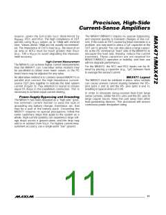
Current-Sense Adjustment
(Resistor Range, Output Adjust)
Choose R
Choos e R
after selecting R
, RG1, and RG2.
OUT
OUT
SENSE
to ob ta in the full-s c a le volta g e you
Note 4: Printed Circuit Design, by Gerald L. Ginsberg; McGraw-Hill, Inc.; page 185.
10 ______________________________________________________________________________________

 MAXIM [ MAXIM INTEGRATED PRODUCTS ]