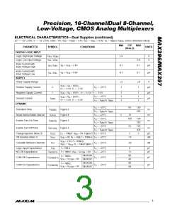
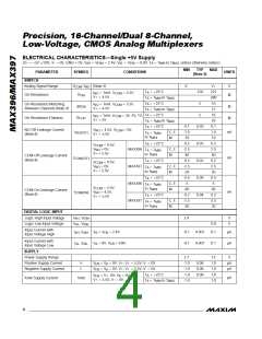
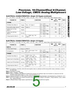
P re c is io n , 1 6 -Ch a n n e l/Du a l 8 -Ch a n n e l,
Lo w -Vo lt a g e , CMOS An a lo g Mu lt ip le x e rs
6/MAX397
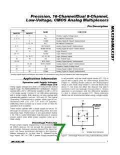
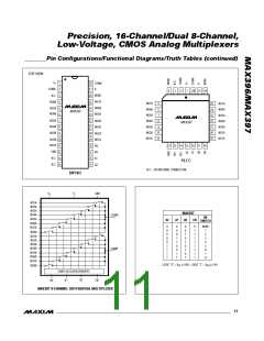
______________________________________________________________P in De s c rip t io n
PIN
NAME
FUNCTION
MAX396
1
MAX397
1
V+
N.C.
Positive Supply-Voltage Input
No Internal Connection
2, 3, 13
—
—
2
3, 13, 14
—
COMB
Analog Signal B Output* (bidirectional)
No Internal Connection
—
N.C.
4–11
—
NO16–NO9
NO8B–NO1B
GND
Analog Signal Inputs* (bidirectional)
Analog Signal B Inputs* (bidirectional)
Logic Ground
4–11
12
12
14–17
—
—
A3–A0
Logic Address Inputs
15, 16, 17
18
A2, A1, A0
EN
Logic Address Inputs
18
Logic Enable Input
19–26
—
—
NO1–NO8
NO1A–NO8A
V-
Analog Signal Inputs* (bidirectional)
Analog Signal A Inputs* (bidirectional)
Negative Supply-Voltage Input
Analog Signal Output* (bidirectional)
Analog Signal A Output* (bidirectional)
19–26
27
27
28
—
COM
—
28
COMA
*Analog signal inputs and outputs are names of convenience only; they are identical and interchangeable.
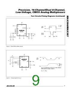
is not possible, add two small-signal diodes (D1, D2) in
__________Ap p lic a t io n s In fo rm a t io n
s e rie s with s up p ly p ins for ove rvolta g e p rote c tion
(Figure 1). Adding diodes reduces the analog-signal
range to one diode drop below V+ and one diode drop
above V-, but does not affect the devices’ low switch
resistance and low leakage characteristics. Device
operation is unchanged, and the difference between
V+ and V- should not exceed 17V. These protection
diodes are not recommended when using a single supply.
Op e ra t io n w it h S u p p ly Vo lt a g e s
Ot h e r t h a n ±5 V
Using supply voltages less than ±5V reduces the analog
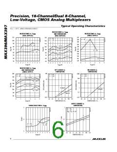
signal range. The MAX396/MAX397 multiplexers (muxes)
operate with ±3V to ±8V bipolar supplies or with a +3V to
+15V single supply. Connect V- to GND when operating
with a single supply. Both devices can also operate with
unbalanced supplies, such as +10V and -5V. The Typical
Op e ra ting Cha ra c te ris tic s g ra p hs s how typ ic a l on-
re s is ta nc e with ± 3V, ± 5V, +3V, a nd +5V s up p lie s .
(Switching times increase by a factor of two or more for
operation at 5V or below.)
+5V
D1
V+
MAX396
MAX397
These muxes operate with a single supply as low as 1V,
although on-resistance and switching times become
extremely high. Performance is not guaranteed below
2.7V. This is useful information only because it assures
proper switch state while power supplies ramp up or
down slowly.
*
*
*
*
NO
COM
Ove rvo lt a g e P ro t e c t io n
Proper power-supply sequencing is recommended for
all CMOS devices. Do not exceed the absolute maxi-
mum ratings, because stresses beyond the listed rat-
ings can cause permanent damage to the devices.
Always sequence V+ on first, then V-, followed by the
logic inputs, NO, or COM. If power-supply sequencing
V-
D2
*INTERNAL PROTECTION DIODES
-5V
Figure 1. Overvoltage Protection Using External Blocking Diodes
_______________________________________________________________________________________
7

 MAXIM [ MAXIM INTEGRATED PRODUCTS ]