P re c is io n , 1 6 -Ch a n n e l/Du a l 8 -Ch a n n e l,
Lo w -Vo lt a g e , CMOS An a lo g Mu lt ip le x e rs
6/MAX397
ELECTRICAL CHARACTERISTICS—Single +5V Supply (continued)
(V+ = +5V ±10%, V- = 0V, GND = 0V, V = V
= 2.4V, V = V
= 0.8V, T = T
to T , unless otherwise noted.)
MAX
AH
ENH
AL
ENL
A
MIN
MIN
TYP
(Note 2)
MAX
PARAMETER
DYNAMIC
SYMBOL
CONDITIONS
UNITS
T
= +25°C
105
245
350
A
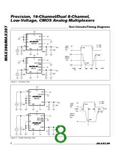
Transition Time (Note 3)
t
V
= 3V, Figure 2
ns
ns
ns
NO
TRANS
T
A
= T to T
MIN MAX
Break-Before-Make Interval
t
(Note 3)
T
A
= +25°C
= +25°C
10
65
OPEN
T
A
125
200
275
125
200
Enable Turn-On Time
(Note 3)
t
ON(EN)
T
A
= T
to T
MIN
MAX
MAX
T
A
= +25°C
100
1.5
Enable Turn-Off Time
(Note 3)
t
ns
OFF(EN)
T
A
= T
to T
MIN
C
= 100pF, V = 0V,
NO
L
Charge Injection (Note 3)
V
CTE
T
A
= +25°C
5
pC
Figure 5
ELECTRICAL CHARACTERISTICS—Single +3V Supply
(V+ = +3V ±10%, V- = 0V, GND = 0V, V = V
= 2.4V, V = V
= 0.8V, T = T
to T , unless otherwise noted.)
MAX
AH
ENH
AL
ENL
A
MIN
MIN
TYP
(Note 2)
MAX
PARAMETER
SWITCH
SYMBOL
CONDITIONS
UNITS
Analog Signal Range
V
(Note 3)
= 1mA, V
V-
V+
V
ANALOG
T
= +25°C
315
230
550
650
A
I
NO
= 1.5V,
COM
On-Resistance
R
Ω
ON
V+ = 3V
T
A
= T
to T
MIN
MAX
MAX
DYNAMIC
T
A
= +25°C
575
750
Figure 2, V = 2.4V,
IN
Transition Time (Note 3)
t
ns
ns
TRANS
V
N01
= 1.5V, V
= 0V
N08
T
A
= T
to T
MIN
Figure 3, V
= 2.4V,
= 1.5V
INH
Enable Turn-On Time (Note 3)
Enable Turn-Off Time (Note 3)
Charge Injection (Note 3)
t
T
A
= +25°C
= +25°C
= +25°C
260
135
1
500
400
5
ON(EN)
V
INL
= 0V, V
N01
Figure 3, V
= 2.4V,
= 1.5V
INH
t
T
A
ns
OFF(EN)
V
INL
= 0V, V
N01
C
= 100pF, V = 0V,
L
NO
V
CTE
T
A
pC
Figure 5
Note 2: The algebraic convention, where the most negative value is a minimum and the most positive value a maximum, is used in
this data sheet.
Note 3: Guaranteed by design.
Note 4: ∆R
= R
- R
.
ON
ON(MAX)
ON(MIN)
Note 5: Flatness is defined as the difference between the maximum and minimum value of on-resistance as measured over the
specified analog signal ranges, i.e., V = 3V to 0V and 0V to -3V.
NO
Note 6: Leakage parameters are 100% tested at maximum rated hot operating temperature, and guaranteed by correlation at +25°C.
Note 7: Worst-case isolation is on channel 4 because of its proximity to the COM pin. Off-isolation = 20log V
/V , V
COM NO COM
= output,
V
NO
= input to off switch.
Note 8: Leakage testing at single supply is guaranteed by correlation testing with dual supplies.
_______________________________________________________________________________________
5

 MAXIM [ MAXIM INTEGRATED PRODUCTS ]