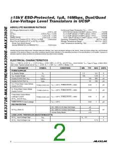
±±15k EꢀDꢁ-rotected, ±µA, ±6Mbps, Dual/Quad
Lowꢁkoltage Level Translators in UCꢀ-
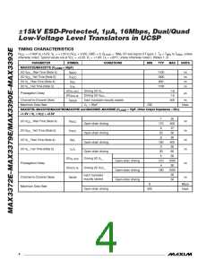
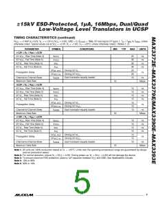
TIMING CHARACTERISTICS (continued)
(V
= +1.65V to +5.5V, V = +1.2V to (V
+ 0.3V), GND = 0, R
= 1MΩ, I/O test signal of Figure 1, T = T
to T
, unless
MAX
CC
L
CC
LOAD
A
A
MIN
otherwise noted. Typical values are at V
= +3.3V, V = +1.8V, T = +25°C, unless otherwise noted.) (Notes 1, 2)
CC
L
PARAMETER
+1.2V ≤ V ≤ V ≤ +3.3V
SYMBOL
CONDITIONS
MIN
TYP
MAX
UNITS
L
CC
I/O V _ Rise Time (Note 4)
t
25
30
30
30
20
20
10
ns
ns
ns
ns
CC
RVCC
I/O V _ Fall Time (Note 5)
t
CC
FVCC
I/O V _ Rise Time (Note 4)
t
RVL
L
I/O V _ Fall Time (Note 5)
L
t
FVL
I/O
I/O
Driving I/O V _
L
VL-VCC
VCC-VL
SKEW
Propagation Delay
ns
Driving I/O V
_
CC
Each translator equally loaded
Channel-to-Channel Skew
Maximum Data Rate
t
ns
10
Mbps
+2.5V ≤ V ≤ V
≤ +3.3V
L
CC
I/O V _ Rise Time (Note 4)
t
15
15
15
15
15
15
10
ns
ns
ns
ns
CC
RVCC
I/O V _ Fall Time (Note 5)
t
CC
FVCC
I/O V _ Rise Time (Note 4)
t
RVL
L
I/O V _ Fall Time (Note 5)
L
t
FVL
I/O
I/O
Driving I/O V _
L
VL-VCC
VCC-VL
SKEW
Propagation Delay
ns
Driving I/O V
_
CC
Channel-to-Channel Skew
Maximum Data Rate
t
Each translator equally loaded
ns
16
Mbps
+1.8V ≤ V ≤ V
≤ +2.5V
L
CC
I/O V _ Rise Time (Note 4)
t
15
15
15
15
15
15
10
ns
ns
ns
ns
CC
RVCC
I/O V _ Fall Time (Note 5)
t
CC
FVCC
I/O V _ Rise Time (Note 4)
t
RVL
L
I/O V _ Fall Time (Note 5)
L
t
FVL
I/O
I/O
Driving I/O V _
L
VL-VCC
VCC-VL
SKEW
Propagation Delay
ns
Driving I/O V
_
CC
Channel-to-Channel Skew
Maximum Data Rate
t
Each translator equally loaded
ns
16
Mbps
Note 1: All units are 100% production tested at T = +25°C. Limits over the operating temperature range are guaranteed by design
A
and not production tested.
Note 2: For normal operation, ensure V < (V
+ 0.3V). During power-up, V > (V
+ 0.3V) will not damage the device.
L
CC
L
CC
Note 3: To ensure maximum ESD protection, place a 1µF capacitor between V
and GND. See Applications Circuits.
CC
Note 4: 10% to 90%
Note 5: 90% to 10%
_______________________________________________________________________________________
5

 MAXIM [ MAXIM INTEGRATED PRODUCTS ]