±±15k EꢀDꢁ-rotected, ±µA, ±6Mbps, Dual/Quad
Lowꢁkoltage Level Translators in UCꢀ-
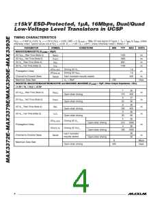
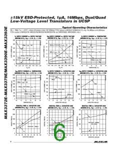
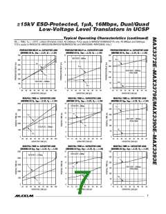
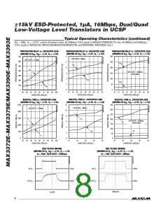
TIMING CHARACTERISTICS
(V
= +1.65V to +5.5V, V = +1.2V to (V
+ 0.3V), GND = 0, R
= 1MΩ, I/O test signal of Figure 1, T = T
to T
, unless
MAX
CC
L
CC
LOAD
A
A
MIN
otherwise noted. Typical values are at V
= +3.3V, V = +1.8V, T = +25°C, unless otherwise noted.) (Notes 1, 2)
CC
L
PARAMETER
SYMBOL
= 50pF)
CONDITIONS
MIN
TYP
MAX
UNITS
MAX3372E/MAX3377E (C
LOAD
I/O V _ Rise Time (Note 4)
t
1100
1000
600
ns
ns
ns
ns
CC
RVCC
I/O V _ Fall Time (Note 5)
t
CC
FVCC
I/O V _ Rise Time (Note 4)
t
RVL
L
I/O V _ Fall Time (Note 5)
L
t
1100
FVL
I/O
I/O
Driving I/O V _
1.6
1.6
500
VL-VCC
VCC-VL
SKEW
L
Propagation Delay
µs
Driving I/O V
_
CC
Channel-to-Channel Skew
Maximum Data Rate
t
Each translator equally loaded
C = 25pF
ns
230
kbps
L
MAX3373E–MAX3376E/MAX3378E/MAX3379E and MAX3390E–MAX3393E (C
= 15pF, Driver Output Impedance ≤ 50Ω)
LOAD
+1.2V ≤ V ≤ V
≤ +5.5V
L
CC
7
170
6
25
400
37
I/O V _ Rise Time (Note 4)
t
ns
ns
ns
ns
CC
RVCC
Open-drain driving
Open-drain driving
Open-drain driving
Open-drain driving
I/O V _ Fall Time (Note 5)
t
CC
FVCC
20
8
50
30
I/O V _ Rise Time (Note 4)
t
RVL
L
180
3
400
30
I/O V _ Fall Time (Note 5)
L
t
LFV
30
5
60
30
I/O
I/O
Driving I/O V _
L
VL-VCC
VCC-VL
SKEW
Open-drain driving
Open-drain driving
Open-drain driving
210
4
1000
30
Propagation Delay
ns
ns
Driving I/O V _
CC
190
1000
20
Each translator
equally loaded
Channel-to-Channel Skew
Maximum Data Rate
t
50
8
Mbps
kbps
Open-drain driving
500
4
_______________________________________________________________________________________

 MAXIM [ MAXIM INTEGRATED PRODUCTS ]