±±15k EꢀDꢁ-rotected, ±µA, ±6Mbps, Dual/Quad
Lowꢁkoltage Level Translators in UCꢀ-
ABꢀOLUTE MAXꢂMUM RATꢂNGꢀ
All Voltages Referenced to GND
Continuous Power Dissipation (T = +70°C)
A
V
I/O V
...........................................................................-0.3V to +6V
8-Pin SOT23 (derate 8.9mW/°C above +70°C)...........714mW
3 x 3 UCSP (derate 4.7mW/°C above +70°C) ............379mW
3 x 4 UCSP (derate 6.5mW/°C above +70°C) ............579mW
14-Pin TSSOP (derate 9.1mW/°C above +70°C) ........727mW
Operating Temperature Range ...........................-40°C to +85°C
Storage Temperature Range.............................-65°C to +150°C
Lead Temperature (soldering, 10s) .................................+300°C
CC
......................................................-0.3V to (V
+ 0.3V)
CC_
CC
I/O V ...........................................................-0.3V to (V + 0.3V)
THREE-STATE...............................................-0.3V to (V + 0.3V)
Short-Circuit Duration I/O V , I/O V
Short-Circuit Duration I/O V or I/O V
L_
L
L
to GND...........Continuous
L
CC
to GND
L
CC
Driven from 40mA Source
(except MAX3372E and MAX3377E) .....................Continuous
Stresses beyond those listed under “Absolute Maximum Ratings” may cause permanent damage to the device. These are stress ratings only, and functional
operation of the device at these or any other conditions beyond those indicated in the operational sections of the specifications is not implied. Exposure to
absolute maximum rating conditions for extended periods may affect device reliability.
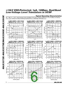
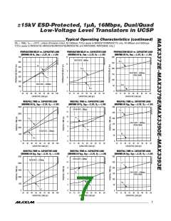
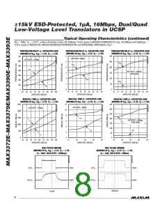
ELECTRꢂCAL CHARACTERꢂꢀTꢂCꢀ
(V
= +1.65V to +5.5V, V = +1.2V to (V
+ 0.3V), GND = 0, I/O V and I/O V
unconnected, T = T
to T
, unless other-
MAX
CC
L
CC
L_
CC_
A
MIN
wise noted. Typical values are at V
= +3.3V, V = +1.8V, T = +25°C.) (Notes 1, 2)
A
L
CC
ꢁARAMETER
ꢀYMBOL
CONDꢂTꢂONꢀ
MꢂN
TYꢁ
MAX
UNꢂTꢀ
ꢁOWER ꢀUꢁꢁLꢂEꢀ
V Supply Range
V
1.2
5.5
5.50
300
100
V
L
L
V
Supply Range
V
1.65
V
CC
CC
Supply Current from V
I
130
16
µA
µA
CC
L
QVCC
Supply Current from V
I
QVL
V
Three-State Output Mode
CC
I
I
T
T
= +25°C, THREE-STATE = GND
= +25°C, THREE-STATE = GND
0.03
0.03
1
1
µA
µA
THREE-STATE-VCC
A
A
Supply Current
V Three-State Output Mode
L
Supply Current
I
THREE-STATE-VL
Three-State Output Mode
Leakage Current
I/O V and I/O V
T
T
= +25°C, THREE-STATE = GND
= +25°C
0.02
0.02
1
1
µA
µA
THREE-STATE-LKG
A
A
L_
CC_
THREE - S TATE Pin Input Leakage
EꢀD ꢁROTECTꢂON
IEC 1000-4-2 Air-Gap Discharge
IEC 1000-4-2 Contact Discharge
Human Body Model
8
8
I/O V
(Note 3)
kV
CC
15
LOGꢂC-LEVEL THREꢀHOLDꢀ (MAX3372E/MAX3377E)
I/O V Input Voltage High
V
V - 0.2
L
V
V
L_
IHL
I/O V Input Voltage Low
V
0.15
L_
ILL
2
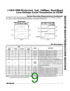
_______________________________________________________________________________________

 MAXIM [ MAXIM INTEGRATED PRODUCTS ]