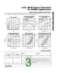
3 .6 V, 1 W RF P o w e r Tra n s is t o rs
fo r 9 0 0 MHz Ap p lic a t io n s
1/MAX602
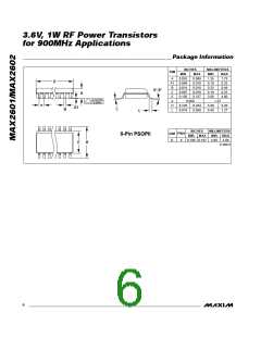
S lu g La yo u t Te c h n iq u e s
__________Ap p lic a t io n s In fo rm a t io n
The mos t imp orta nt c onne c tion to ma ke to the
MAX2601/MAX2602 is the back side. It should connect
directly to the PC board ground plane if it is on the top
side, or through numerous plated through-holes if the
ground plane is buried. For maximum gain, this con-
nection should have very little self-inductance. Since it
is also the thermal path for heat dissipation, it must
have low thermal impedance, and the ground plane
should be large.
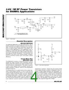
Op t im u m P o rt Im p e d a n c e
The source and load impedances presented to the
MAX2601/MAX2602 have a direct impact upon its gain,
output power, and linearity. Proper source- and load-
terminating impedances (Z and Z ) presented to the
S
L
power transistor base and collector will ensure optimum
performance.
For a power transistor, simply applying the conjugate of
the transistor’s input and output impedances calculated
from small-signal S-parameters will yield less than opti-
mum device performance.
For maximum efficiency at V
= 0.75V and V
=
BB
CC
3.6V, the optimum power-transistor source and load
impedances (as defined in Figure 3) are:
4
3
2
1
At 836MHz: Z = 5.5 + j2.0
S
Z = 6.5 + j1.5
MAX2601
MAX2602
L
2.8nH
2.8nH
2.8nH
At 433MHz: Z = 9.5 - j2.5
S
Z = 8.5 - j1.5
L
Z
and Z reflect the impedances that should be pre-
L
S
sented to the transistor’s base and collector. The pack-
age parasitics are dominated by inductance (as shown
in Figure 3), and need to be accounted for when calcu-
2.8nH
Z
S
Z
L
lating Z and Z .
S
L
The internal bond and package inductances shown
in Figure 3 should be included as part of the end-
application matching network, depending upon exact
layout topology.
5
6
7
8
Figure 3. Optimum Port Impedance
_______________________________________________________________________________________
5

 MAXIM [ MAXIM INTEGRATED PRODUCTS ]