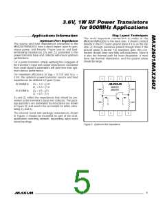
3 .6 V, 1 W RF P o w e r Tra n s is t o rs
fo r 9 0 0 MHz Ap p lic a t io n s
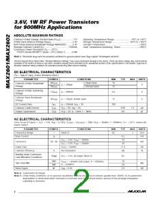
ABSOLUTE MAXIMUM RATINGS
Collector-Emitter Voltage, Shorted Base (V
)....................17V
Operating Temperature Range ...........................-40°C to +85°C
Storage Temperature Range .............................-65°C to +165°C
Junction Temperature ......................................................+150°C
Lead Temperature (soldering, 10sec) .............................+300°C
CES
Emitter Base Reverse Voltage (V
)...................................2.3V
EBO
BIAS Diode Reverse Breakdown Voltage (MAX2602) ..........2.3V
Average Collector Current (I )........................................1200mA
C
Continuous Power Dissipation (T = +70°C)
A
PSOPII (derate 80mW/°C above +70°C) (Note 1) ..........6.4W
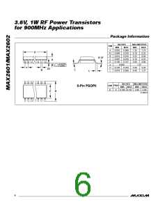
Note 1: Backside slug must be properly soldered to ground plane (see Slug Layout Techniques section).
Stresses beyond those listed under “Absolute Maximum Ratings” may cause permanent damage to the device. These are stress ratings only, and functional
operation of the device at these or any other conditions beyond those indicated in the operational sections of the specifications is not implied. Exposure to
absolute maximum rating conditions for extended periods may affect device reliability.
DC ELECTRICAL CHARACTERISTICS
(T = T
to T , unless otherwise noted.)
MAX
A
MIN
PARAMETER
SYMBOL
BV
CONDITIONS
Open base
Shorted base
MIN
15
TYP
MAX
UNITS
CEO
Collector-Emitter Breakdown
Voltage
I
C
< 100µA
V
BV
15
CES
1/MAX602
Collector-Emitter Sustaining
Voltage
LV
I
= 200mA
5.0
V
V
CEO
C
Collector-Base Breakdown
Voltage
BV
I
C
< 100µA, emitter open
15
CBO
DC Current Gain
h
I
C
= 250mA, V = 3V
100
FE
CE
Collector Cutoff Current
Output Capacitance
I
V
= 6V, V = 0V
0.05
9.6
1.5
µA
pF
CES
CE
BE
C
V
= 3V, I = 0mA, f = 1MHz
OB
CB E
AC ELECTRICAL CHARACTERISTICS
(Test Circuit of Figure 1, V = 3.6V, V = 0.750V, Z
= Z
= 50Ω, P
= 30dBm, f = 836MHz, T = +25°C, unless oth-
OUT A
CC
BB
LOAD
SOURCE
erwise noted.)
PARAMETER
SYMBOL
CONDITIONS
MIN
TYP
MAX
UNITS
GHz
Frequency Range
Base Current
f
(Note 2)
DC
1
I
B
4.2
-43
-42
11.6
58
mA
V
= 3.6V, P
= 3.0V, P
= 30dBm
= 29dBm
dBc
dBc
CC
OUT
OUT
Harmonics
2fo, 3fo
V
CC
Power Gain
P
= 30dBm
dB
%
OUT
η
Collector Efficiency
No modulation
Stability under Continuous
Load Mismatch Conditions
V
SWR
V
CC
= 5.5V, all angles (Note 3)
8:1
IM3
IM5
NF
-16
-25
3.3
P
= +30dBm total power, f1 = 835MHz,
OUT
Two-Tone IMR
dBc
dB
f2 = 836MHz
V = 0.9V
BB
Noise Figure
Note 2: Guaranteed by design.
Note 3: Under these conditions: a) no spurious oscillations shall be observed at collector greater than -60dBc; b) no parametric
degradation is observable when mismatch is removed; and c) no current draw in excess of the package dissipation
capability is observed.
2
_______________________________________________________________________________________

 MAXIM [ MAXIM INTEGRATED PRODUCTS ]