3 .6 V, 1 W RF P o w e r Tra n s is t o rs
fo r 9 0 0 MHz Ap p lic a t io n s
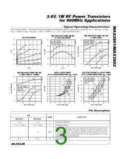
V
CC
V
BB
5Ω
1000pF
0.1µF
L1
0.1µF
1000pF
24Ω
100nH
1000pF
1
8
4
5
T2
1000pF
RF
IN
10pF
2pF
T1
2, 6, 7
BACKSIDE
SLUG
2pF
12pF
L1 = COILCRAFT A05T INDUCTOR, 18.5nH
T1, T2 = 1", 50Ω TRANSMISSION LINE ON FR-4
1/MAX602
Figure 1. Test Circuit
_______________De t a ile d De s c rip t io n
MAX2 6 0 1 /MAX2 6 0 2
The MAX2601/MAX2602 are high-performance silicon
bipolar transistors in power-enhanced, 8-pin SO pack-
ages. The base and collector connections use two pins
each to reduce series inductance. The emitter con-
nects to three (MAX2602) or four (MAX2601) pins in
addition to a back-side heat slug, which solders direct-
ly to the PC board ground to reduce emitter inductance
and improve thermal dissipation. The transistors are
intended to be used in the common-emitter configura-
tion for ma ximum p owe r g a in a nd p owe r-a d d e d
efficiency.
V
CC
V
CC
R
BIAS
RF
C
RF
OUT
C
OUT
RF
C
Q1
Q2
C
BIAS
Cu rre n t Mirro r Bia s
(MAX2 6 0 2 o n ly)
C
IN
The MAX2602 inc lud e s a hig h-p e rforma nc e s ilic on
bipolar RF power transistor and a thermally matched
biasing diode that matches the power transistor’s ther-
mal and process characteristics. This diode is used to
c re a te a b ia s ne twork tha t a c c ura te ly c ontrols the
power transistor’s collector current as the temperature
changes (Figure 2).
RF
IN
Figure 2. Bias Diode Application
temperature variations. Simply tying the biasing diode
to the supply through a resistor is adequate in most sit-
uations. If large supply variations are anticipated, con-
nect the biasing diode to a reference voltage through a
resistor, or use a stable current source. Connect the
biasing diode to the base of the RF power transistor
through a large RF impedance, such as an RF choke
(inductor), and decouple to ground through a surface-
mount chip capacitor larger than 1000pF.
The biasing diode is a scaled version of the power tran-
sistor’s base-emitter junction, in such a way that the
current through the biasing diode is 1/15 the quiescent
collector current of the RF power transistor. Supplying
the biasing diode with a constant current source and
connecting the diode’s anode to the RF power transis-
tor’s base ensures that the RF power transistor’s quies-
c e nt c olle c tor c urre nt re ma ins c ons ta nt throug h
4
_______________________________________________________________________________________

 MAXIM [ MAXIM INTEGRATED PRODUCTS ]