Low Supply Current, Step-Up DC-DC Converters
with True-Shutdown
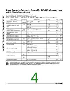
Pin Description
PIN
NAME
FUNCTION
Low-Battery Comparator Input. Internally set to trip at +0.85V. This function remains operational in
shutdown.
±
LBI
Dual-Mode™ Feedback Input. Connect to GND for preset 5.0V output. Connect to OUT for preset
3.3V output. Connect a resistive voltage-divider from OUT to GND to adjust the output voltage from
2V to 5.5V.
2
FB
Low-Battery Comparator Output, Open-Drain Output. LBO is low when V
remains operational in shutdown.
< 0.85V. This function
LBI
3
4
LBO
Shutdown Input. If SHDN is high, the device is in shutdown mode, OUT is high impedance, and
LBI/LBO are still operational. Connect shutdown to GND for normal operation.
SHDN
5
6
7
8
GND
LX
Ground
Inductor Connection
OUT
BATT
Power Output. OUT provides bootstrap power to the IC.
Battery Input and Damping Switch Connection
Detailed Description
V
IN
The MAX±795/MAX±796/MAX±797 compact step-up
DC-DC converters start up with voltages as low as
0.85V and operate with an input voltage down to +0.7V.
Consuming only 25µA of quiescent current, these
devices have an internal synchronous rectifier that
reduces cost by eliminating the need for an external
diode and improves overall efficiency by minimizing
losses in the circuit (see Synchronous Rectification sec-
tion for details). The internal N-channel MOSFET power
switch resistance is typically 0.±7Ω, which minimizes
losses. The LX switch current limits of the MAX±795/
MAX±796/MAX±797 are 0.25A, 0.5A, and ±A, respec-
tively.
22µH
47µF
1M
BATT
LX
SHDN
LBO
V
= 3.3V
OUT
OUT
MAX1795
MAX1796
MAX1797
C
*
OUT
V
IN
GND
FB
LBI
*SEE TABLE 1 FOR COMPONENT VALUES.
All three devices offer Maxim’s proprietary True-
Shutdown circuitry, which disconnects the output from
the input in shutdown and puts the output in a high
impedance state. These devices also feature Maxim’s
proprietary LX-damping circuitry, which reduces EMI in
noise-sensitive applications. For additional in-system
flexibility, the LBI/LBO comparator remains active in
shutdown. (Figure ± is a typical application circuit).
Figure 1. Typical Application Circuit
rent of a traditional pulse-skipping controller (Figure 2).
Switching frequency depends upon the load current
and input voltage, and can range up to 500kHz. Unlike
conventional pulse-skipping DC-DC converters (where
ripple amplitude varies with input voltage), ripple in
these devices does not exceed the product of the
switch current limit and the filter-capacitor equivalent
series resistance (ESR).
Control Scheme
A unique minimum-off-time, current-limited control
scheme is the key to the MAX±795/MAX±796/
MAX±797s’ low operating current and high efficiency
over a wide load range. The architecture combines the
high output power and efficiency of a pulse-width-mod-
ulation (PWM) device with the ultra-low quiescent cur-
Dual Mode is a trademark of Maxim Integrated Products.
8
_______________________________________________________________________________________

 MAXIM [ MAXIM INTEGRATED PRODUCTS ]