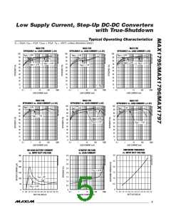
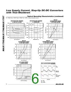
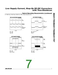
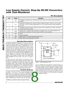
Low Supply Current, Step-Up DC-DC Converters
with True-Shutdown
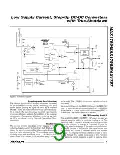
pate this energy, minimizing the ringing at LX.
V
IN
Damping LX ringing does not reduce V
does reduce EMI (Figures 3, 4, and 5).
ripple, but
OUT
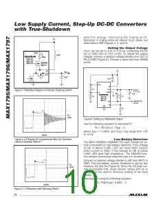
Setting the Output Voltage
can be set to 3.3V or 5.0V by connecting the FB
V
OUT
BATT
pin to GND (5V) or OUT (3.3V). To adjust the output
voltage, connect a resistive voltage-divider from OUT to
FB to GND (Figure 6). Choose a value less than 250kΩ
for R2.
R1
22µH
200Ω
MAX1795
MAX1796
MAX1797
DAMPING
SWITCH
V
IN
LX
V
OUT
OUT
47µF
47µF
BATT
LBI
LX
R3
R4
OUT
OUTPUT
Figure 3. Simplified Diagram of Inductor Damping Switch
2V TO 5.5V
SHDN
1M
47µF
R1
R2
MAX1795
MAX1796
MAX1797
LOW-BATTERY
OUTPUT
LBO
FB
GND
V
LX
1V/div
Figure 6. Setting an Adjustable Output
Use the following equation to calculate R±:
R± = R2 [(V
/ V ) - ±]
FB
OUT
where V = +±.245V, and V
FB
may range from +2V
OUT
to +5.5V.
2µs/div
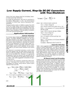
Figure 4. LX Ringing for Conventional Step-Up Converter
(without Damping Switch)
Low-Battery Detection
The MAX±795/MAX±796/MAX±797 each contain an on-
chip comparator for low-battery detection. If the voltage
at LBI is above 0.85V, LBO (an open-drain output)
sinks current to GND. If the voltage at LBI is below
0.85V, LBO goes high impedance. The LBI/LBO func-
tion remains active even when the part is in shutdown.
Connect a resistive voltage-divider to LBI from BATT to
GND. The low-battery monitor threshold is set by two
resistors, R3 and R4 (Figure 6). Since the LBI bias cur-
rent is typically 2nA, large resistor values (R4 up to
250kΩ) can be used to minimize loading of the input
supply.
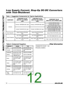
V
LX
1V/div
Calculate R3 using the following equation:
R3 = R4[(V
/ 0.85V) - ±]
TRIP
2µs/div
Figure 5. LX Waveform with Damping Switch
10 ______________________________________________________________________________________

 MAXIM [ MAXIM INTEGRATED PRODUCTS ]