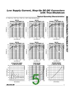
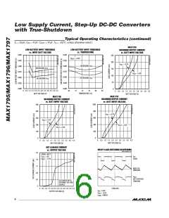
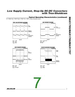
Low Supply Current, Step-Up DC-DC Converters
with True-Shutdown
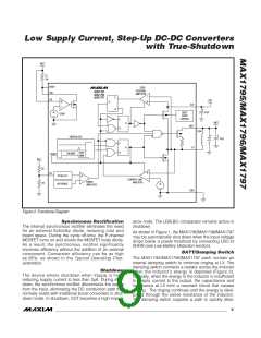
V
is the input voltage where the low-battery detec-
TRIP
I
RIP
tor output goes high impedance.
I
= I
LIM
−
(±− D)
OUT(MAX)
2
For single-cell applications, LBI may be connected to
the battery. When V
<±.0V>, the LBI threshold
BATT
increases to 0.925V (see Typical Operating Char-
acteristics).
where: I
I
= Inductor ripple current (A)
RIP
V
= Output voltage (V)
OUT
Connect a pullup resistor of ±00kΩ or greater from LBO
to OUT for a logic output. LBO is an open-drain output
and can be pulled as high as 6V regardless of the volt-
age at OUT. When LBI is below the threshold, the LBO
output is high impedance. If the low-battery comparator
is not used, ground LBI and LBO.
= Device current limit (0.25A, 0.5A, or ±A)
LIM
R
= On-resistance of P-channel MOSFET
PFET
(Ω) (typ 0.27Ω)
L
= ESR of Inductor (Ω) (typ 0.095Ω)
ESR
V
= Input voltage (V)
BATT
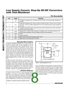
Applications Information
L = Inductor value in µH
= LX switch’s off-time (µs) (typ ±µs)
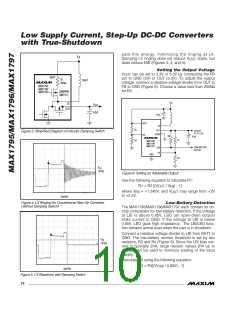
Inductor Selection
An inductor value of 22µH performs well in most appli-
cations. The MAX±795/MAX±796/MAX±797 will also
work with inductors in the ±0µH to 47µH range. Smaller
inductance values typically offer a smaller physical size
for a given series resistance, allowing the smallest
overall circuit dimensions, but have lower output cur-
rent capability. Circuits using larger inductance values
exhibit higher output current capability, but are physi-
cally larger for the same series resistance and current
rating.
t
OFF
D = Duty cycle
R
= On-resistance of N-channel MOSFET
NFET
(Ω) (typ 0.±7Ω)
I
= Maximum output current (A)
OUT(MAX)
Capacitor Selection
Table ± lists suggested tantalum or polymer capacitor
values for typical applications. The ESR of both input
bypass and output filter capacitors affects efficiency
and output ripple. Output voltage ripple is the product
of the peak inductor current and the output capacitor
ESR. High-frequency output noise can be reduced by
connecting a 0.±µF ceramic capacitor in parallel with
the output filter capacitor. (See Table 2 for a list of sug-
gested component suppliers.)
The inductor’s incremental saturation current rating
should be greater than the peak switch-current limit,
which is 0.25A for the MAX±795, 0.5A for the MAX±796,
and ±A for the MAX±797. However, it is generally
acceptable to bias the inductor into saturation by as
much as 20% although this will slightly reduce efficien-
cy. Table ± lists some suggested components for typi-
cal applications.
PC Board Layout and Grounding
Careful printed circuit layout is important for minimizing
ground bounce and noise. Keep the IC’s GND pin and
the ground leads of the input and output filter capaci-
tors less than 0.2in (5mm) apart. In addition, keep all
connections to the FB and LX pins as short as possible.
In particular, when using external feedback resistors,
locate them as close to FB as possible. To maximize
output power and efficiency and minimize output ripple
voltage, use a ground plane and solder the IC’s GND
pin directly to the ground plane.
The inductor’s DC resistance significantly affects effi-
ciency. Calculate the maximum output current
(I
RIP
) as follows, using inductor ripple current
OUT(MAX)
(I ) and duty cycle (D):
V
+ I
× (R
+ L
)− V
ESR BATT
OUT
LIM
L
PFET
I
=
RIP
(R
+ L
)
ESR
PFET
+
t
2
OFF
I
RIP
2
V
+
I
−
(R
+ L
)− V
ESR BATT
OUT
LIM
PFET
D =
and
I
RIP
V
+
I
−
(R
− R
+ L
)
ESR
OUT
LIM
PFET
NFET
2
______________________________________________________________________________________ 11

 MAXIM [ MAXIM INTEGRATED PRODUCTS ]