Notebook CPU Step-Down Controller for Intel
-
Mobile Voltage Positioning (IMVP II)
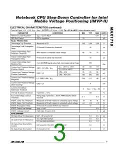
ELECTRICAL CHARACTERISTICS (continued)
(Circuit of Figure 1, V+ = 15V, V
= V
= SKP/SDN = 5V, V
= 1.25V, T = -40°C to +85°C, unless otherwise noted.) (Note 2)
OUT A
CC
DD
PARAMETER
CONDITIONS
MIN
TYP
MAX UNITS
TON = V , open, or REF (200kHz, 300kHz, or 550kHz)
CC
500
ns
Minimum Off-Time (Note 1)
TON = GND (1000kHz)
375
BIAS AND REFERENCE
Quiescent Supply Current (V
Quiescent Supply Current (V
)
)
Measured at V , FB forced above the regulation point
1300
5
µA
µA
CC
CC
Measured at V , FB forced above the regulation point
DD
DD
Quiescent Battery Supply
Current (V+)
40
µA
Shutdown Supply Current (V
)
5
5
µA
µA
SKP/SDN = 0
SKP/SDN = 0
CC
Shutdown Supply Current (V
)
DD
Shutdown Battery Supply
Current (V+)
5
µA
V
SKP/SDN = 0, V
= V
= 0 or 5V
CC
DD
Reference Voltage
V
CC
= 4.5V to 5.5V, no REF load
1.98
2.02
FAULT PROTECTION
Overvoltage Trip Threshold
Measured at FB
1.95
65
2.05
75
V
Output Undervoltage Protection
Threshold
With respect to unloaded output voltage
%
Current-Limit Threshold Voltage
(Positive, Default)
GND - LX, ILIM = V
GND - LX
80
115
mV
mV
mV
V
CC
ILIM = 0.5V
33
65
Current-Limit Threshold Voltage
(Positive, Adjustable)
ILIM = REF (2V)
160
240
Current-Limit Threshold Voltage
(Negative)
LX - GND, ILIM = V
-145
4.1
-90
4.4
CC
V
CC
Undervoltage Lockout
Rising edge, hysteresis = 20mV, PWM disabled below this
level
Threshold
VGATE Lower Trip Threshold
VGATE Upper Trip Threshold
GATE DRIꢁERS
Measured at FB with respect to unloaded output voltage
Measured at FB with respect to unloaded output voltage
-12.5
+7.5
-7.5
%
%
+12.5
DH Gate Driver On-Resistance
BST - LX forced to 5V
DL, high state (pullup)
DL, low state (pulldown)
3.5
3.5
1.0
Ω
Ω
DL Gate Driver On-Resistance
_______________________________________________________________________________________
5

 MAXIM [ MAXIM INTEGRATED PRODUCTS ]