Notebook CPU Step-Down Controller for Intel
-
Mobile Voltage Positioning (IMVP II)
ABSOLUTE MAXIMUM RATINGS
V+ to GND..............................................................-0.3V to +30V
LX to BST..................................................................-6V to +0.3V
REF Short Circuit to GND...........................................Continuous
Continuous Power Dissipation
28-Pin QSOP (derate 10.8mW/°C above +70°C).........860mW
Operating Temperature Range ..........................-40°C to +85°C
Junction Temperature......................................................+150°C
Storage Temperature.........................................-65°C to +150°C
Lead Temperature (soldering, 10s) .................................+300°C
V
, V
to GND .....................................................-0.3V to +6V
CC DD
D0–D4, ZMODE, VGATE, OVP, SUS, to GND .........-0.3V to +6V
SKP/SDN to GND ...................................................-0.3V to +16V
ILIM, CC, REF, POS, NEG, S1, S0,
TON, TIME to GND.................................-0.3V to (V
DL to GND..................................................-0.3V to (V
BST to GND............................................................-0.3V to +36V
DH to LX .....................................................-0.3V to (BST + 0.3V)
+ 0.3V)
+ 0.3V)
CC
DD
Stresses beyond those listed under “Absolute Maximum Ratings” may cause permanent damage to the device. These are stress ratings only, and functional
operation of the device at these or any other conditions beyond those indicated in the operational sections of the specifications is not implied. Exposure to
absolute maximum rating conditions for extended periods may affect device reliability.
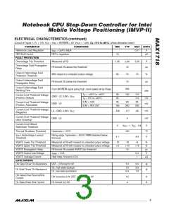
ELECTRICAL CHARACTERISTICS
(Circuit of Figure 1, V+ = 15V, V = V = SKP/SDN = 5V, V
= 1.25V, T = 0°C to +85°C, unless otherwise noted.)
A
CC
DD
OUT
PARAMETER
CONDITIONS
MIN
TYP
MAX UNITS
PWM CONTROLLER
Battery voltage, V+
2
28
V
Input Voltage Range
V , V
CC DD
4.5
5.5
V+ = 4.5V to 28V,
includes load
regulation error
DAC codes from 0.9V to 1.75V
DAC codes from 0.6V to 0.875V
-1
+1
%
%
DC Output Voltage Accuracy
-1.5
+1.5
Line Regulation Error
Input Bias Current
V
= 4.5V to 5.5V, V
= 4.5V to 28V
5
mV
µA
V
CC
BATT
FB, POS, NEG
-0.2
0.4
+0.2
2.5
POS, NEG Common-Mode Range
POS, NEG Differential Range
POS, NEG Offset Gain
POS - NEG
-80
0.81
-8
+80
0.91
+8
mV
V/V
∆V / (POS - NEG); POS - NEG = 50mV
150kHz nominal, R
380kHz nominal, R
0.86
FB
= 120kΩ
= 47kΩ
TIME
TIME Frequency Accuracy
-12
-12
230
165
320
465
+12
+12
290
215
390
565
500
375
%
TIME
38kHz nominal, R
= 470kΩ
TIME
V+ = 5V, FB = 1.2V, TON = GND (1000kHz)
TON = REF (550kHz)
TON = open (300kHz)
TON = V (200kHz)
260
190
355
515
400
300
On-Time (Note 1)
ns
ns
V+ = 12V, FB = 1.2V
CC
TON = V , open, or REF (200kHz, 300kHz, or 550kHz)
CC
Minimum Off-Time (Note 1)
TON = GND (1000kHz)
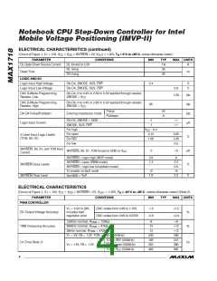
BIAS AND REFERENCE
Quiescent Supply Current (V
Quiescent Supply Current (V
)
)
Measured at V , FB forced above the regulation point
700
<1
1200
5
µA
µA
CC
CC
Measured at V , FB forced above the regulation point
DD
DD
Quiescent Battery Supply
Current (V+)
25
40
µA
Shutdown Supply Current (V
)
2
5
5
µA
µA
SKP/SDN = GND
SKP/SDN = GND
CC
Shutdown Supply Current (V
)
<1
DD
Shutdown Battery Supply
Current (V+)
<1
2
5
µA
V
SKP/SDN = GND, V
= V
= 0V or 5V
CC
DD
Reference Voltage
V
CC
= 4.5V to 5.5V, no REF load
1.98
2.02
2
_______________________________________________________________________________________

 MAXIM [ MAXIM INTEGRATED PRODUCTS ]