Complete, Isolated RS-485/RS-422
Data Interface
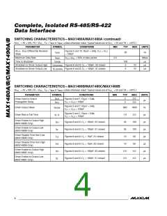
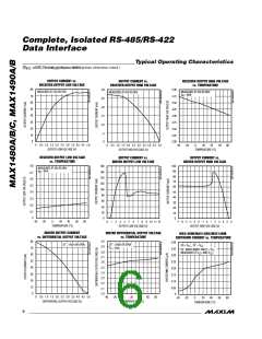
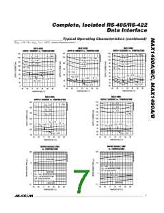
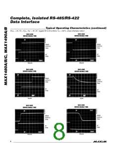
SWITCHING CHARACTERISTICS—MAX1480B/MAX1480C/MAX1490B (continued)
(V
CC_
= 5V 10ꢀ, FS = V
, T = T
to T
, unless otherwise noted. Typical values are at V
= 5V and TA = +25°C.)
CC_
A
MIN
MAX
CC_
PARAMETER
SYMBOL
CONDITIONS
MIN
TYP
MAX
UNITS
Driver Disable Time from Low
(MAX1480C Only)
t
LZ
Figures 6 and 8, C = 15pF, S1 closed
2.0
4.5
µs
L
Driver Disable Time from High
(MAX1480C Only)
t
Figures 6 and 8, C = 15pF, S2 closed
2.0
4.5
µs
µs
ns
HZ
L
t
t
2
2
3.0
3.0
PLH
Receiver Input to Output
Propagation Delay
Figures 5 and 10, R
= 54Ω,
= 54Ω,
DIFF
C
= C = 100pF
L2
L1
PHL
|t
- t
| Differential Receiver
Figures 5 and 10, R
= C = 100pF
PLH PHL
DIFF
t
1200
SKD
Skew
C
L1
L2
Maximum Data Rate
f
t
, t
< 50ꢀ of data period
0.25
Mbps
µs
MAX
PLH PHL
Time to Shutdown
t
100
35
SHDN
Shutdown to Driver Output High
Shutdown to Driver Output Low
t
Figures 6 and 9, C = 100pF, S2 closed
100
100
µs
ZH(SHDN)
L
t
Figures 6 and 9, C = 100pF, S1 closed
35
µs
ZL(SHDN)
L
Note 1: All currents into device pins are positive; all currents out of device pins are negative. All voltages are referenced to logic-
side ground (GND_), unless otherwise specified.
Note 2: For DE´ and DI´ pin descriptions, see Detailed Block Diagram and Typical Application Circuit (Figure 1 for MAX1480A/
MAX1480B/MAX1480C, Figure 2 for MAX1490A/MAX1490B).
Note 3: Shutdown supply current is the current at V
and V
when shutdown is enabled.
CC1
CC2
Note 4: Applies to peak current (see Typical Operating Characteristics). Although the MAX1480A/B/C and MAX1490A/B provide
electrical isolation between logic ground and signal paths, they do not provide isolation between external shields and the
signal paths (see Isolated Common Connection section).
_______________________________________________________________________________________
5

 MAXIM [ MAXIM INTEGRATED PRODUCTS ]