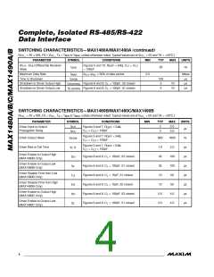
Complete, Isolated RS-485/RS-422
Data Interface
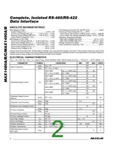
ABSOLUTE MAXIMUM RATINGS
With Respect to GND_
LED Forward Current (DI, DE, ISO RO LED) ......................50mA
Supply Voltage (V
Control Input Voltage (SD, FS)...............-0.3V to (V
Receiver Output Voltage (RO, RO)........-0.3V to (V
Output Switch Voltage (D1, D2)........................................+12V
With Respect to ISO COM_
Control Input Voltage (ISO DE_ )....-0.3V to (ISO V
Driver Input Voltage (ISO DI_ ) .......-0.3V to (ISO V
Receiver Output Voltage (ISO RO_) ...-0.3V to (ISO V
)...........................................-0.3V to +6V
Continuous Power Dissipation (T = +70°C)
CC_
A
+ 0.3V)
+ 0.3V)
24-Pin Plastic DIP (derate 8.7mW°C above +70°C) .....696mW
28-Pin Plastic DIP (derate 9.09mW/°C above +70°C) ..727mW
Operating Temperature Ranges
MAX1480_CPI/MAX1490_CPG............................0°C to +70°C
MAX1480_EPI/MAX1490_EPG .........................-40°C to +85°C
Storage Temperature Range.............................-65°C to +160°C
Lead Temperature (soldering, 10s) .................................+300°C
CC_
CC_
+ 0.3V)
+ 0.3V)
+ 0.3V)
CC_
CC_
CC_
Driver Output Voltage (A, B, Y, Z ) ......................-8V to +12.5V
Receiver Input Voltage (A, B)..............................-8V to +12.5V
Stresses beyond those listed under “Absolute Maximum Ratings” may cause permanent damage to the device. These are stress ratings only, and functional
operation of the device at these or any other conditions beyond those indicated in the operational sections of the specifications is not implied. Exposure to
absolute maximum rating conditions for extended periods may affect device reliability.
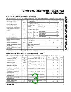
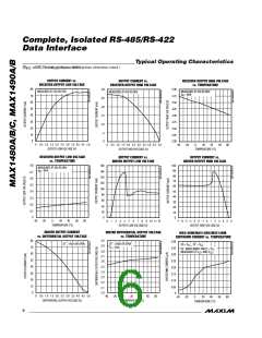
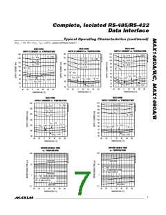
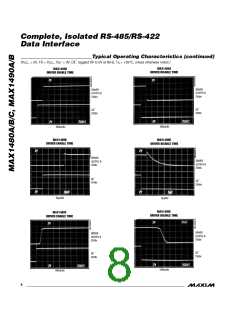
ELECTRICAL CHARACTERISTICS
(V
CC_
= 5V 10ꢀ, V = V
FS
, T = T
to T
, unless otherwise noted. Typical values are at V = 5V and T = +25°C.) (Notes 1, 2)
MAX CC_ A
CC_
A
MIN
PARAMETER
SYMBOL
CONDITIONS
MIN
TYP
535
725
60
MAX
UNITS
f
V
= 0V
FS
SWL
Switch Frequency
kHz
f
FS = V
or open
CC_
SWH
R = ∞, +25°C only
L
90
45
MAX1480A,
DE´ = V
or open
or open
or open
CC_
R = 54Ω
120
35
L
R = ∞, +25°C only
L
MAX1480B,
DE´ = V
CC_
R = 54Ω
L
95
R = ∞, +25°C only
L
35
75
MAX1480C,
DE´ = V
Operating Supply Current
I
mA
CC
CC_
R = 54Ω
L
95
R = ∞, +25°C only
100
170
65
150
125
L
MAX1490A
MAX1490B
R = 54Ω
L
R = ∞, +25°C only
L
R = 54Ω
L
130
Shutdown Supply Current
(Note 3)
I
SD = V
0.2
µA
SHDN
CC_
V
High
Low
2.4
2.4
SDH
Shutdown Input Threshold
V
pA
V
V
0.8
SDL
Shutdown Input Leakage Current
FS Input Threshold
10
V
High
Low
FSH
V
0.8
50
FSL
FS Input Pullup Current
FS Input Leakage Current
Input High Voltage
FS low
µA
pA
V
FS high
DE´, DI´
DE´, DI´
10
V
V
- 0.4
CC_
IH
Input Low Voltage
V
0.4
8
V
IL
Isolation Resistance
Isolation Capacitance
R
C
T
A
T
A
= +25°C, V
= 50VDC
100
10,000
10
MΩ
pF
ISO
ISO
ISO
ISO
= +25°C, V
= 50VDC
Differential Driver Output
(No Load)
V
V
OD1
2
_______________________________________________________________________________________

 MAXIM [ MAXIM INTEGRATED PRODUCTS ]