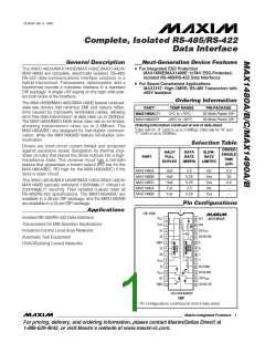
Complete, Isolated RS-485/RS-422
Data Interface
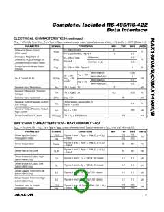
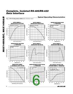
ELECTRICAL CHARACTERISTICS (continued)
(V
CC_
= 5V 10ꢀ, V = V
FS
, T = T
to T
, unless otherwise noted. Typical values are at V
= 5V and T = +25°C.) (Notes 1, 2)
CC_ A
CC_
A
MIN
MAX
PARAMETER
SYMBOL
CONDITIONS
R = 50Ω (RS-422)
MIN
2
TYP
MAX
UNITS
Differential Driver Output
(With Load)
V
V
OD2
R = 27Ω (RS-485), Figure 4
1.5
5.0
0.3
Change in Magnitude of
Differential Output Voltage for
Complementary Output States
Differential
R = 27Ω or 50Ω,
∆V
V
V
OD
Figure 4
Common mode
0.3
4
Driver Common-Mode Output
Voltage
V
R = 27Ω or 50Ω, Figure 4
OC
MAX1490A/B
0.25
1
V
V
= 12V
= -7V
IN
IN
DE´ = 0V,
= 0V
or 5.5V
MAX1480A/B/C
MAX1490A/B
V
Input Current (A, B)
ISO I
mA
CC_
IN
0.2
0.8
MAX1480A/B/C
Receiver Input Resistance
R
-7V ≤ V
-7V ≤ V
≤ 12V
≤ 12V
12
kΩ
V
IN
CM
CM
Receiver Differential Threshold
Voltage
V
-0.2
+0.2
TH
Receiver Input Hysteresis
∆V
V
= 0V
CM
70
mV
V
TH
OL
Receiver Output/Receiver Output
Low Voltage
Using resistor values listed in
Tables 1 and 2
V
0.4
Receiver Output/Receiver Output
High Current
I
V
= 5.5V
OUT
250
µA
OH
Driver Short-Circuit Current
ISO I
-7V ≤ V ≤ 12V (Note 4)
100
mA
OSD
O
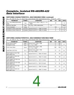
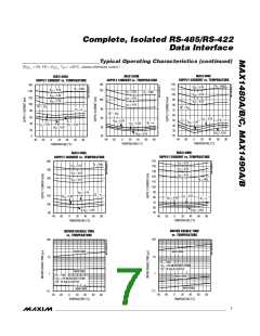
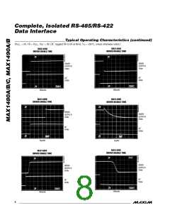
SWITCHING CHARACTERISTICS—MAX1480A/MAX1490A
(V
CC_
= 5V 10ꢀ, FS = V
, T = T
to T
, unless otherwise noted. Typical values are at V
= 5V and TA = +25°C.)
CC_
A
MIN
MAX
CC_
PARAMETER
SYMBOL
CONDITIONS
MIN
TYP
100
100
MAX
275
UNITS
t
t
PLH
PHL
Driver Input to Output
Propagation Delay
Figures 5 and 7, R
= 100pF
= 54Ω, C = C
L1
DIFF
DIFF
DIFF
L2
L2
L2
ns
275
Figures 5 and 7, R
= 100pF
= 54Ω, C = C
L1
Driver Output Skew
t
25
15
90
40
ns
ns
µs
µs
µs
µs
ns
SKEW
Figures 5 and 7, R
= 100pF
= 54Ω, C = C
L1
Driver Rise or Fall Time
t
t
R, F
Driver Enable to Output High
(MAX1480A Only)
t
Figures 6 and 8, C = 100pF, S2 closed
0.2
0.2
0.2
0.2
1.5
1.5
1.5
1.5
ZH
L
Driver Enable to Output Low
(MAX1480A Only)
t
Figures 6 and 8, C = 100pF, S1 closed
L
ZL
LZ
HZ
Driver Disable Time from Low
(MAX1480A Only)
t
Figures 6 and 8, C = 15pF, S1 closed
L
Driver Disable Time from High
(MAX1480A Only)
t
Figures 6 and 8, C = 15pF, S2 closed
L
t
100
100
225
225
PLH
Receiver Input to Output
Propagation Delay
Figures 5 and 10, R = 54Ω, C = C
DIFF L1 L2
= 100pF
t
PHL
_______________________________________________________________________________________
3

 MAXIM [ MAXIM INTEGRATED PRODUCTS ]