MAX14586/MAX14590
High-Current Overvoltage Protectors
with Adjustable OVLO
R
C
R
D
1MΩ
1.5kΩ
I
100%
90%
PEAK-TO-PEAK RINGING
(NOT DRAWN TO SCALE)
I
P
R
DISCHARGE
RESISTANCE
CHARGE-CURRENT-
LIMIT RESISTOR
AMPERES
HIGH-
VOLTAGE
DC
DEVICE
UNDER
TEST
36.8%
C
100pF
s
STORAGE
CAPACITOR
10%
0
SOURCE
TIME
t
0
t
RL
DL
CURRENT WAVEFORM
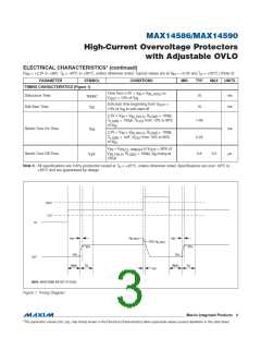
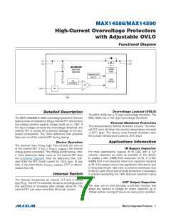
Figure 2a. Human Body ESD Test Model
Figure 2b. Human Body Current Waveform
External OVLO Adjustment Functionality
If OVLO is connected to ground, the internal OVLO com-
parator uses the internally set OVLO value.
Ordering Information/
Selector Guide
If an external resistor-divider is connected to OVLO and
TOP
MARK
OVLO
(V)
PART
PIN-PACKAGE
V
OVLO
exceeds the OVLO select voltage (V
)
OVLO_SELECT ,
the internal OVLO comparator reads the IN fraction fixed
by the external resistor-divider.
MAX14586ETA+T
MAX145ꢀ0ETA+T
8 TDFN-EP*
8 TDFN-EP*
BNJ
BNK
7
15
R1 = 1MI is a good starting value for minimum current
Note: All devices are specified over the -40°C to +85°C oper-
ating temperature range.
+Denotes a lead(Pb)-free/RoHS-compliant package.
T = Tape and reel.
consumption. Since V
, V
, and
IN_OVLO
OVLO_THRESH
R1 are known, R2 can be calculated from the following
formula:
R1
R2
*EP = Exposed pad.
V
= V
× 1+
IN_OVLO
OVLO_THRESH
Chip Information
This external resistor-divider is completely independent
from the internal resistor-divider.
PROCESS: BiCMOS
ESD Test Conditions
ESD performance depends on a number of conditions.
Package Information
The devices are specified for Q15kV (HBM) typical ESD
resistance on IN when IN is bypassed to ground with a
1FF ceramic capacitor.
For the latest package outline information and land patterns
(footprints), go to www.maxim-ic.com/packages. Note that a
“+”, “#”, or “-” in the package code indicates RoHS status only.
Package drawings may show a different suffix character, but
the drawing pertains to the package regardless of RoHS status.
Human Body Model ESD Protection
Figure 2a shows the HBM and Figure 2b shows the
current waveform it generates when discharged into a
low-impedance state. This model consists of a 100pF
capacitor charged to the ESD voltage of interest, which is
then discharged into the device through a 1.5kIresistor.
PACKAGE
TYPE
PACKAGE
CODE
OUTLINE
NO.
LAND
PATTERN NO.
8 TDFN-EP
T822+2
21-0168
ꢀ0-0065
����������������������������������������������������������������� Maxim Integrated Products
8

 MAXIM [ MAXIM INTEGRATED PRODUCTS ]