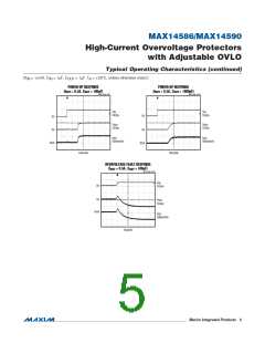
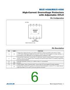
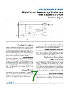
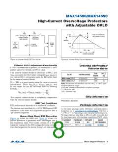
MAX14586/MAX14590
High-Current Overvoltage Protectors
with Adjustable OVLO
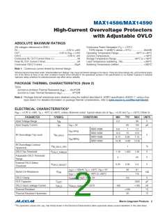
ABSOLUTE MAXIMUM RATINGS
(All voltages referenced to GND.)
Continuous Power Dissipation (T = +70NC)
A
IN...........................................................................-0.3V to +40V
TDFN (derate 11.9mW/NC above +70NC)....................954mW
Operating Temperature Range.......................... -40NC to +85NC
Junction Temperature .....................................................+150NC
Storage Temperature Range............................ -65NC to +150NC
Lead Temperature (soldering, 10s) ................................+300NC
Soldering Temperature (reflow) ......................................+260NC
OUT ............................................................-0.3V to (V + 0.3V)
IN
OVLO.......................................................................-0.3V to +6V
Continuous IN, OUT Current (Note 1).....................................3A
Peak IN, OUT Current (10ms).................................................5A
Continuous OVLO Current ..................................................50FA
Note 1: Continuous current limited by thermal design.
Stresses beyond those listed under “Absolute Maximum Ratings” may cause permanent damage to the device. These are stress ratings only, and functional opera-
tion of the device at these or any other conditions beyond those indicated in the operational sections of the specifications is not implied. Exposure to absolute
maximum rating conditions for extended periods may affect device reliability.
PACKAGE THERMAL CHARACTERISTICS (Note 2)
TDFN
Junction-to-Ambient Thermal Resistance (B ) .......83.9NC/W
JA
Junction-to-Case Thermal Resistance (B ).............. 37NC/W
JC
Note 2: Package thermal resistances were obtained using the method described in JEDEC specification JESD51-7, using a four-
layer board. For detailed information on package thermal considerations, refer to www.maxim-ic.com/thermal-tutorial.
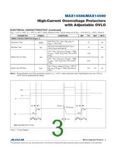
ELECTRICAL CHARACTERISTICS
(V = +2.2V to +36V, T = -40NC to +85NC, unless otherwise noted. Typical values are at V = +5.0V and T = +25NC.) (Note 3)
IN
A
IN
A
PARAMETER
SYMBOL
CONDITIONS
MIN
TYP
MAX
36
UNITS
V
Input Voltage Range
Input Supply Current
V
2.2
IN
I
V
V
< 5V
65
7
120
FA
IN
IN
MAX14586
6.8
14.5
6.73
14.35
7.2
rising
IN
MAX14590
MAX14586
MAX14590
15
15.5
7.13
15.35
IN Overvoltage Trip Level
V
V
IN_OVLO
6.93
14.85
V
falling
IN
IN Overvoltage Lockout
Hysteresis
V
1
%
V
IN_OVLO_HYS
OVLO Set Threshold
V
1.18
4
1.223
1.26
20
OVLO_THRESH
Adjustable OVLO Threshold
Range
V
External OVLO Select
Threshold
V
0.25
0.35
48
0.4
V
OVLO_SELECT
I
I
I
= 100mA, T = +25°C, V = 5V
81
OUT
A
IN
Switch On-Resistance
R
mI
ON
= 100mA, T = -40°C to +85°C
115
OUT
A
OVLO Clamp
= 10FA, V = 5V
3.6
V
CLAMP
IN
OUT Capacitor
C
1000
+100
FF
nA
NC
NC
OUT
OVLO Input Leakage Current
Thermal Shutdown
I
V
= 1.221V
-100
OVLO
OVLO_THRESH
+150
20
Thermal Shutdown Hysteresis
����������������������������������������������������������������� Maxim Integrated Products
2
*The parametric values (min, typ, max limits) shown in the Electrical Characteristics table supersede values quoted elsewhere in this data sheet.

 MAXIM [ MAXIM INTEGRATED PRODUCTS ]