Half-Duplex RS-485-/RS-422-Compatible
Transceiver with AutoDirection Control
AꢁSOLUTE MAXIMUM RATINGS
(All voltages referenced to GND.)
Operating Temperature Range ...........................-40°C to +85°C
Supply Voltage V ...............................................................+6V
Junction Temperature......................................................+150°C
Storage Temperature Range.............................-65°C to +150°C
Lead Temperature (soldering 10s) ..................................+300°C
CC
SHDN, RE, DI..............................................................-0.3V to +6
A, ꢂ........................................................................... -8V to +13V
Short-Circuit Duration (RO, A, ꢂ) to GND ..................Continuous
Continuous Power Dissipation (T = +70°C)
A
8-Pin SO (derate 5.9mW/°C above +70°C)..................471mW
Stresses beyond those listed under “Absolute Maximum Ratings” may cause permanent damage to the device. These are stress ratings only, and functional
operation of the device at these or any other conditions beyond those indicated in the operational sections of the specifications is not implied. Exposure to
absolute maximum rating conditions for extended periods may affect device reliability.
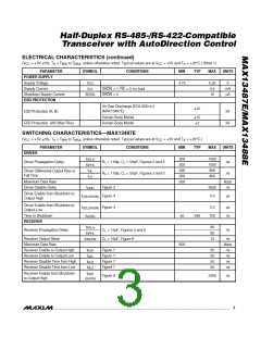
ELECTRICAL CHARACTERISTICS
(V
= +5V 5ꢃ, T = T
to T
, unless otherwise noted. Typical values are at V
= +5V and T = +25°C.) (Note 1)
CC A
CC
A
MIN
MAX
PARAMETER
SYMꢁOL
CONDITIONS
MIN
TYP
MAX
UNITS
DRIVER
R
R
= 100Ω, Figure 1
2.0
1.5
V
V
DIFF
CC
Differential Driver Output
V
V
= 54Ω, Figure 1
V
V
OD
OC
DIFF
No load
CC
3
Driver Common-Mode Output
Voltage
R = 100Ω or 54Ω, Figure 1
L
V
/ 2
CC
Driver Disable Threshold
Input-ꢁigh Voltage
Input-Low Voltage
Input Current
V
Figure 2 (Note 2)
DI, SHDN, RE
DI, SHDN, RE
DI, SHDN, RE
+0.6
2.0
+1
V
V
DT
V
Iꢁ
V
0.8
1
V
IL
I
µA
IN
Driver Short-Circuit Output
Current
(Note 3)
0V ≤ V
≤ +12V
≤ 0V
+50
+250
-50
OUT
I
mA
mA
OSD
-7V ≤ V
-250
20
OUT
(V
CC
- 1V) ≤ V
≤ +12V
OUT
Driver Short-Circuit Foldbacꢀ
Output Current (Note 3)
I
OSDF
-7V ≤ V
≤ 0V
-20
OUT
RECEIVER
V
V
= +12V
= -7V
250
IN
IN
Input Current
(A and ꢂ)
DI = V , V
CC CC
= GND or +5V
I
µA
A, ꢂ
-200
-200
Receiver Differential Threshold
Voltage
V
-7V ≤ V ≤ +12V
+200
mV
mV
V
Tꢁ
CM
Receiver Input ꢁysteresis
Output-ꢁigh Voltage
Output-Low Voltage
∆V
V
+ V = 0V
25
Tꢁ
A
ꢂ
V
-
CC
V
I
= -1.6mA, V - V > V
O A ꢂ Tꢁ
Oꢁ
1.5
V
I
O
= 1mA, V - V < -V
0.4
1
V
OL
A
ꢂ
Tꢁ
Tri-State Output Current at
Receiver
I
0V ≤ V ≤ V
µA
ꢀΩ
mA
OZR
O
CC
Receiver Input Resistance
R
-7V ≤ V
≤ +12V
48
7
IN
CM
Receiver Output Short-Circuit
Current
I
0V ≤ V
≤ V
CC
95
OSR
RO
2
_______________________________________________________________________________________

 MAXIM [ MAXIM INTEGRATED PRODUCTS ]