Half-Duplex RS-485-/RS-422-Compatible
Transceiver with AutoDirection Control
important factor when sizing these resistors is to guar-
Detailed Description
antee that the idle voltage on the bus (A-ꢂ) is greater
than 200mV in order to remain compatible with stan-
dard RS-485 receiver thresholds.
The MAX13487E/MAX13488E half-duplex, high-speed
transceivers for RS-485/RS-422 communication contain
one driver and one receiver. The MAX13487E/
MAX13488E feature a hot-swap capability allowing line
insertion without erroneous data transfer (see the Hot-
Swap Capability section). The MAX13487E features
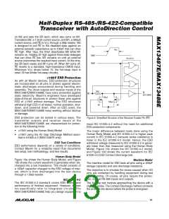
reduced slew-rate drivers that minimize EMI and
reduce reflections caused by improperly terminated
cables, allowing error-free transmission up to 500ꢀbps.
The MAX13488E driver slew rate is not limited, maꢀing
data throughput of up to 16Mbps possible.
Idle State
When not transmitting data, the MAX13487E/
MAX13488E require the DI input be driven high to
remain in the idle state. A conventional RS-485 trans-
ceiver has DE and RE inputs that are used to enable
and disable the driver and receiver. ꢁowever, the
MAX13487E/MAX13488E does not have a DE input,
and instead uses an internal state machine to enable
and disable the drivers. DI must be driven high in order
to go to the idle state.
AutoDirection Circuitry
Internal circuitry in the MAX13487E/MAX13488E, in
conjunction with an external pullup resistor on A and
pulldown resistor on ꢂ (see Typical Operation Circuit),
act to automatically disable or enable the driver and
receiver to ꢀeep the bus in the correct state. This
AutoDirection circuitry consists of a state machine and
an additional receive comparator that determines
whether this device is trying to drive the bus, or another
node on the networꢀ is driving the bus.
Hot-Swap Capability
Hot-Swap Inputs
When circuit boards are inserted into a hot or powered
bacꢀ plane, differential disturbances to the data bus
can lead to data errors. Upon initial circuit-board inser-
tion, the data communication processor undergoes its
own power-up sequence. During this period, the
processor’s logic-output drivers are high impedance
and are unable to drive the DI and RE inputs of these
devices to a defined logic level. Leaꢀage currents up to
10µA from the high-impedance state of the proces-
sor’s logic drivers could cause standard CMOS enable
inputs of a transceiver to drift to an incorrect logic level.
Additionally, parasitic circuit-board capacitance could
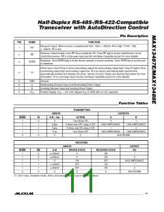
The internal state machine has two inputs:
• DI
• The current state of A-ꢂ (determined by a dedicated
differential comparator)
The state machine also has two outputs:
cause coupling of V
or GND to the enable inputs.
• DRIVER_ENAꢂLE—Internal signal that enables and
disables the driver
CC
Without the hot-swap capability, these factors could
improperly enable the transceiver’s driver.
• RECEIVER_ENAꢂLE—Internal signal that is the
inverse of the DRIVER_ENAꢂLE signal, but it can be
overridden by an external pin
To overcome both these problems, two different pullup
switches (strong and weaꢀ) are turned on during the
power-up. When V
rises, an internal power-up signal
CC
When DI is low, the device always drives the bus low.
When DI is high, the device drives the bus for a short
time, then disables the driver and allows the external
pullup/pulldown resistors to hold the bus in the high
state (A-ꢂ > 200mV). During each low-to-high transition
of DI, the driver stays enabled until (A-ꢂ) > V , and
DT
then disables the driver, letting the pullup/pulldown
resistors hold the A and ꢂ lines in the correct state.
enables a strong pullup circuit. It holds DI and RE high
with 1mA for 15µs. Once the timeout is expired, this
strong pullup is switched off. A weaꢀ pullup (100µA)
remains active to overcome leaꢀage on the pin. This
second weaꢀ pullup disappears as soon as the micro-
controller forces a low state on these pins. Therefore, in
normal operation (after the first activation), these pins
can be considered as high-impedance pins (CMOS
inputs) without any pullup circuitry.
Pullup and Pulldown Resistors
The pullup and pulldown resistors on the A and ꢂ lines
are required for proper operation of the device
although their exact value is not critical. They function
to hold the bus in the high state (A-ꢂ > 200mV) follow-
ing a low-to-high transition. Sizing of these resistors is
determined in the same way as when using any other
RS-485 driver and depends on how the line is terminat-
ed and how many nodes are on the bus. The most
The AutoDirection state machine is initialized, forcing the
driver disabled. The receiver is enabled in AutoDirection
mode.
Hot-Swap Input Circuitry
The enable inputs feature hot-swap capability. At the
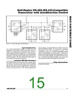
input there are two pMOS devices, M1 and M2 (Figure 9).
When V
ramps from zero, an internal 15µs timer turns
CC
12 ______________________________________________________________________________________

 MAXIM [ MAXIM INTEGRATED PRODUCTS ]