DS1302 Trickle-Charge Timekeeping Chip
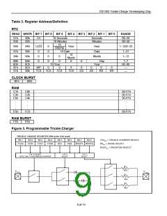
CLOCK/CALENDAR BURST MODE
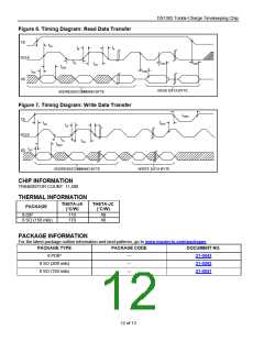
The clock/calendar command byte specifies burst mode operation. In this mode, the first eight clock/calendar
registers can be consecutively read or written (see Table 3) starting with bit 0 of address 0.
If the write-protect bit is set high when a write clock/calendar burst mode is specified, no data transfer will occur to
any of the eight clock/calendar registers (this includes the control register). The trickle charger is not accessible in
burst mode.
At the beginning of a clock burst read, the current time is transferred to a second set of registers. The time
information is read from these secondary registers, while the clock may continue to run. This eliminates the need to
re-read the registers in case of an update of the main registers during a read.
RAM
The static RAM is 31 x 8 bytes addressed consecutively in the RAM address space.
RAM BURST MODE
The RAM command byte specifies burst mode operation. In this mode, the 31 RAM registers can be consecutively
read or written (see Table 3) starting with bit 0 of address 0.
REGISTER SUMMARY
A register data format summary is shown in Table 3.
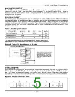
CRYSTAL SELECTION
A 32.768kHz crystal can be directly connected to the DS1302 via pins 2 and 3 (X1, X2). The crystal selected for
use should have a specified load capacitance (CL) of 6pF. For more information on crystal selection and crystal
layout consideration, refer to Application Note 58: Crystal Considerations for Dallas Real-Time Clocks.
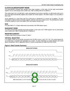
Figure 4. Data Transfer Summary
SINGLE-BYTE READ
CE
SCLK
I/O
R/W A0 A1 A2 A3 A4 R/C
1
D0 D1 D2 D3 D4 D5 D6 D7
SINGLE-BYTE WRITE
CE
SCLK
I/O
R/W A0 A1 A2 A3 A4 R/C
1
D0 D1 D2 D3 D4 D5 D6 D7
NOTE: IN BURST MODE, CE IS KEPT HIGH AND ADDITIONAL SCLK CYCLES ARE SENT UNTIL THE END OF THE BURST.
8 of 13

 MAXIM [ MAXIM INTEGRATED PRODUCTS ]