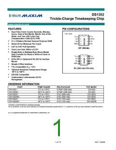
DS1302 Trickle-Charge Timekeeping Chip
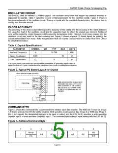
OSCILLATOR CIRCUIT
The DS1302 uses an external 32.768kHz crystal. The oscillator circuit does not require any external resistors or
capacitors to operate. Table 1 specifies several crystal parameters for the external crystal. Figure 1 shows a
functional schematic of the oscillator circuit. If using a crystal with the specified characteristics, the startup time is
usually less than one second.
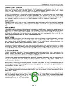
CLOCK ACCURACY
The accuracy of the clock is dependent upon the accuracy of the crystal and the accuracy of the match between
the capacitive load of the oscillator circuit and the capacitive load for which the crystal was trimmed. Additional
error will be added by crystal frequency drift caused by temperature shifts. External circuit noise coupled into the
oscillator circuit may result in the clock running fast. Figure 2 shows a typical PC board layout for isolating the
crystal and oscillator from noise. Refer to Application Note 58: Crystal Considerations for Dallas Real-Time Clocks
for detailed information.
Table 1. Crystal Specifications*
PARAMETER
Nominal Frequency
Series Resistance
Load Capacitance
SYMBOL
MIN
TYP
MAX
UNITS
kHz
kΩ
fO
ESR
CL
32.768
45
6
pF
*The crystal, traces, and crystal input pins should be isolated from RF generating signals. Refer to
Application Note 58: Crystal Considerations for Dallas Real-Time Clocks for additional specifications.
Figure 2. Typical PC Board Layout for Crystal
LOCAL GROUND PLANE (LAYER 2)
X1
NOTE: AVOID ROUTING SIGNALS IN THE
CROSSHATCHED AREA (UPPER LEFT-
CRYSTAL
HAND QUADRANT) OF THE PACKAGE
X2
UNLESS THERE IS A GROUND PLANE
BETWEEN THE SIGNAL LINE AND THE
PACKAGE.
GND
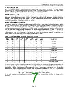
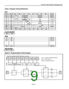
COMMAND BYTE
Figure 3 shows the command byte. A command byte initiates each data transfer. The MSB (bit 7) must be a logic
1. If it is 0, writes to the DS1302 will be disabled. Bit 6 specifies clock/calendar data if logic 0 or RAM data if logic 1.
Bits 1 to 5 specify the designated registers to be input or output, and the LSB (bit 0) specifies a write operation
(input) if logic 0 or read operation (output) if logic 1. The command byte is always input starting with the LSB (bit 0).
Figure 3. Address/Command Byte
7
1
6
5
4
3
2
1
0
RAM
CK
RD
W R
A4
A3
A2
A1
A0
5 of 13

 MAXIM [ MAXIM INTEGRATED PRODUCTS ]