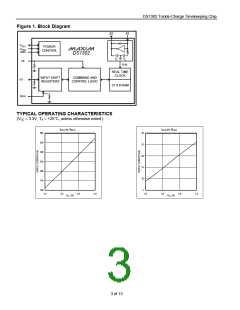
DS1302 Trickle-Charge Timekeeping Chip
CLOCK HALT FLAG
Bit 7 of the seconds register is defined as the clock halt (CH) flag. When this bit is set to logic 1, the clock oscillator
is stopped and the DS1302 is placed into a low-power standby mode with a current drain of less than 100nA. When
this bit is written to logic 0, the clock will start. The initial power-on state is not defined.
WRITE-PROTECT BIT
Bit 7 of the control register is the write-protect bit. The first seven bits (bits 0 to 6) are forced to 0 and always read 0
when read. Before any write operation to the clock or RAM, bit 7 must be 0. When high, the write-protect bit
prevents a write operation to any other register. The initial power-on state is not defined. Therefore, the WP bit
should be cleared before attempting to write to the device.
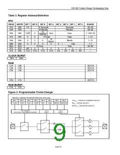
TRICKLE-CHARGE REGISTER
This register controls the trickle-charge characteristics of the DS1302. The simplified schematic of Figure 5 shows
the basic components of the trickle charger. The trickle-charge select (TCS) bits (bits 4 to 7) control the selection of
the trickle charger. To prevent accidental enabling, only a pattern of 1010 enables the trickle charger. All other
patterns will disable the trickle charger. The DS1302 powers up with the trickle charger disabled. The diode select
(DS) bits (bits 2 and 3) select whether one diode or two diodes are connected between VCC2 and VCC1. If DS is 01,
one diode is selected or if DS is 10, two diodes are selected. If DS is 00 or 11, the trickle charger is disabled
independently of TCS. The RS bits (bits 0 and 1) select the resistor that is connected between VCC2 and VCC1. The
resistor and diodes are selected by the RS and DS bits as shown in Table 2.
Table 2. Trickle Charger Resistor and Diode Select
TCS
BIT 7
TCS
BIT 6
TCS
BIT 5
TCS
BIT 4
DS
BIT 3
DS
BIT 2
RS
BIT 1
RS
BIT 0
FUNCTION
X
X
X
1
1
1
1
1
1
0
X
X
X
0
0
0
0
0
0
1
X
X
X
1
1
1
1
1
1
0
X
X
X
0
0
0
0
0
0
1
X
0
1
0
0
0
1
1
1
1
X
0
1
1
1
1
0
0
0
1
0
X
X
0
1
1
0
1
1
0
0
X
X
1
0
1
1
0
1
0
Disabled
Disabled
Disabled
1 Diode, 2kΩ
1 Diode, 4kΩ
1 Diode, 8kΩ
2 Diodes, 2kΩ
2 Diodes, 4kΩ
2 Diodes, 8kΩ
Initial power-on state
Diode and resistor selection is determined by the user according to the maximum current desired for battery or
super cap charging. The maximum charging current can be calculated as illustrated in the following example.
Assume that a system power supply of 5V is applied to VCC2 and a super cap is connected to VCC1. Also assume
that the trickle charger has been enabled with one diode and resistor R1 between VCC2 and VCC1. The maximum
current IMAX would therefore be calculated as follows:
IMAX = (5.0V – diode drop) / R1 ≈ (5.0V – 0.7V) / 2kΩ ≈ 2.2mA
As the super cap charges, the voltage drop between VCC2 and VCC1 decreases and therefore the charge current
decreases.
7 of 13

 MAXIM [ MAXIM INTEGRATED PRODUCTS ]