DA9181.006
13 October, 1999
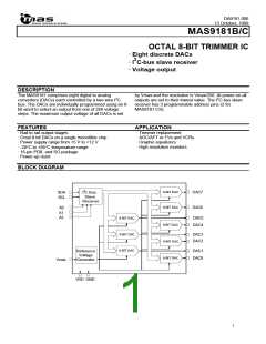
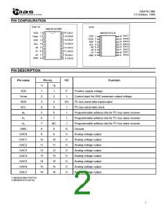
FUNCTIONS
ꢀAddress Byte
Valid addresses are 40, 42, 44, 46, 48, 4A, 4C, 4E(hex),
depending on the programming of bits A2, A1 and A0.
With these addresses, up to eight MAS9181 ICs can be
operated independently from one I2C-bus. No other
addresses are acknowledged by the MAS9181. The
address inputs A0, A1 and A2 are programmed by
connection to GND for An = 0 or to VDD for An = 1. If
the inputs are left floating, An = 1 will result. For
MAS9181CS, A2 is always 1.
ꢀInstruction and data bytes
Valid instructions from 00 to 0F and F0 to FF (hex);
MAS9181 will not respond to other instruction value, but
will still generate an acknowledgement. Instructions 00
to0F cause auto-incrementing of the sub-address (bits
SD to SA) when more than one data byte is sent within
one transmission. With auto-incrementing, the first data
byte is written into the DAC addessed by bits SD to SA
and then the sub-address is automatically incremented
by one position for the next databyte in the series. Auto-
incrementing does not occur with instructions F0 to FF.
The DAC addressed by the sub-address will always
receive the data if more than one data byte is sent.
Valid sub-addresses (bits SD to SA) are 0 to 7 (hex)
relating numerically to DAC0 to DAC7. When the auto-
incrementing function is used, the sub-address will
sequence through all possible values (0 to F, 0 to F,
etc.). While the sub-address is between 8 and F no
DAC outputs change.
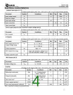
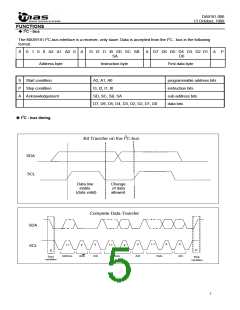
ꢀI2C - bus
Input SCL (pin 4) and input/output SDA (pin 3) conform
to I2C-bus specifications. Pins 3 and 4 are protected
against voltage pulses by internal zener diodes
connected to the ground plane and therefore the normal
bus line voltage shall not exceed 5.5V.
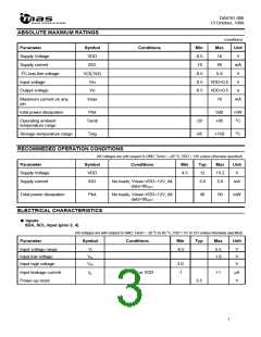
ꢀInput Vmax
Input Vmax (pin 2) provides a means of comprising the
output voltage swing of the DACs. The maximum DAC
output voltage is restricted to approximately Vmax while
the 8-bit resolution is maintained, therefore giving a
finer voltage resolution of smaller output swings.
6

 MAS [ MICRO ANALOG SYSTEMS ]