DA9181.006
13 October, 1999
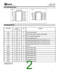
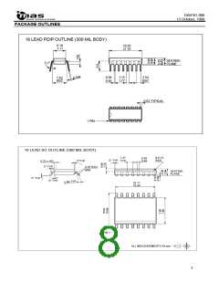
PIN CONFIGURATION
PDIP 16
SO16
MAS9181BN
1
16
VDD
DAC7
MAS9181CS
DAC7
VDD
Vmax
SDA
SCL
NC
A0
16
15
14
13
12
11
10
9
2
3
4
5
6
15 DAC6
14 DAC5
13 DAC4
Vmax
1
2
3
4
5
6
7
DAC6
DAC5
DAC4
DAC3
DAC2
DAC1
DAC0
SDA
SCL
A0
12
11
10
DAC3
DAC2
DAC1
A1
A1
GND
7
8
A2
GND
8
9 DAC0
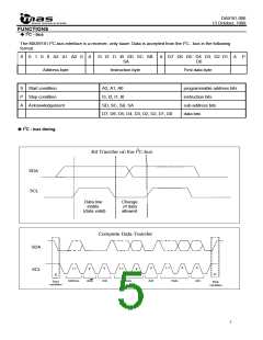
PIN DESCRIPTION
Pin name
Pin no.
I/O
Function
*1
1
2
3
4
5
6
7
8
9
*2
1
VDD
Vmax
SDA
SCL
A0
P
I
Positive supply voltage
2
Control input for DAC maximum output voltage
I2C bus serial data input/output
I2C bus serial data clock
Programmable address bits for I2C bus slave receiver
Programmable address bits for I2C bus slave receiver
Programmable address bits for I2C bus slave receiver
Ground
3
I/O
I
4
6
I
A1
7
I
A2
NC
8
I
GND
DAC0
G
O
O
O
O
O
O
O
O
9
Analog voltage output
DAC1
DAC2
DAC3
DAC4
DAC5
DAC6
DAC7
10
11
12
13
14
15
16
10
11
12
13
14
15
16
Analog voltage output
Analog voltage output
Analog voltage output
Analog voltage output
Analog voltage output
Analog voltage output
Analog voltage output
*1 MAS9181BN (PDIP16)
*2 MAS9181CS (SO16)
2

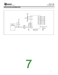
 MAS [ MICRO ANALOG SYSTEMS ]