DA9181.006
13 October, 1999
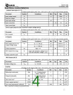
ELECTRICAL CHARACTERISTICS
Address Input (pins 5, 6, 7)
(All voltages are with respect to GND; Tamb = -20 oC to 85 oC; VDD = 5V to 12V unless otherwise specified)
Parameter
Symbol
Conditions
Min
Typ
Max
Unit
Input voltage range
Input low voltage
Input high voltage
VI
0
VDD
1.0
V
V
V
VIL
VIH
3.0
Input current low
IIL
-10
-15
1
µA
µA
Input current high
IIH
Vmax Control Input for DAC maximum output voltage (pin 2)
(All voltages are with respect to GND; Tamb = -20 oC to 85 oC; VDD = 5V to 12V unless otherwise specified)
Parameter
Pin 2 current
ꢀOutputs
Symbol
Conditions
Min
Typ
Max
Unit
I2
7
10
µA
(All voltages are with respect to GND; Tamb = -20 oC to 85 oC; VDD = 5V to 12V unless otherwise specified)
Parameter
Symbol
Conditions
Io = +/- 100 µA
Io = +/- 500 µA
data = 7F
Min
0.1
0.2
Typ
Max
Unit
V
DAC output (pin 9 to 16)
Output voltage range
Vo
VDD-0.1
VDD-0.2
V
Output impedance
Zo
Io
30
Ω
DAC output drive range
Upper side saturation voltage= 0.2v
Low side saturation voltage = 0.2v
-1
1
2
mA
Output capacitive load
Co
nF
SDA Output (pin 3)
(All voltages are with respect to GND; Tamb = -20 oC to 85 oC; VDD = 5V to 12V unless otherwise specified)
Parameter
Symbol
Conditions
Min
Typ
Max
Unit
Output voltage low
VOL
I3 = 3.0 mA
0.4
V
Linearity
(All voltages are with respect to GND; Tamb = -20 oC to 85 oC; VDD = 5V to 12V unless otherwise specified)
Parameter
Symbol
Conditions
Min
Typ
Max
Unit
Differential nonlinearity
DNL
Io = 0 (without load)
Vmax = VDD-1.0
-1
1
LSB
Integral nonlinearity
INL
Io = 0 (without load)
Vmax = VDD-1.0
-1.5
1.5
LSB
Zero code error1
ZCE
PSRR
TCo
data = 00
10
30
5
mV
Power supply rejection1
Zero code temperature coefficient1
mV/V
µV/oC
-200
200
Note 1: Guaranteed by design but not production tested
4

 MAS [ MICRO ANALOG SYSTEMS ]