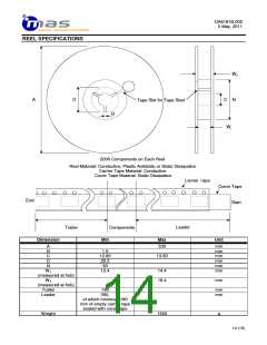
DA6181B.002
5 May, 2011
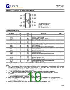
MAS6181 SAMPLES IN PDIP-20 PACKAGE
1
2
3
4
5
20 VSS
19 RFI2
18 RFIM
17 RFIP
16
VDD
QO2
QO1
6
7
8
9
15
QI
AGC
14 PDN1
13 AON
12 DEC
11
Top Marking Definitions:
YYWW = Year Week
XXXXX.X = Lot Number
ZZ = Sample Version
PDN2
OUT 10
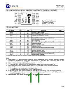
PIN DESCRIPTION
Pin Name
Pin
Type
Function
Note
1
NC
VDD
QO2
QO1
2
3
P
Positive Power Supply
AO
AO
NC
NC
AI
Quartz Filter Output for Crystal 2
Quartz Filter Output for Crystal 1
4
5
1
1
6
QI
7
Quartz Filter Input for Crystal
AGC Capacitor
AGC
PDN2
OUT
8
AO
DI
9
Power Down/Frequency Selection Input 2
Receiver Output
2
3
10
11
12
13
14
15
16
17
18
19
20
DO
NC
AO
DI
DEC
AON
Demodulator Capacitor
AGC On Control
4
2
PDN1
DI
Power Down/Frequency Selection Input 1
NC
NC
AI
RFIP
RFIM
RFI2
VSS
Positive Receiver Input
5
5
AI
Negative Receiver Input
AI
Receiver Input 2 (for Antenna Capacitor 2)
Power Supply Ground
G
A = Analog, D = Digital, P = Power, G = Ground, I = Input, O = Output, NC = Not Connected
Notes:
1) Pins 5 and 6 between QO1 and QI must be connected to VSS to eliminate DIL package lead frame parasitic
capacitances disturbing the crystal filter performance. All other NC (Not Connected) pins are also
recommended to be connected to VSS to minimize noise coupling.
2) PDN1 = VDD and PDN2 = VDD means receiver off
Fast start-up is triggered when the receiver is after power down controlled to power on
-
3) OUT = VSS when carrier amplitude at maximum; OUT = VDD when carrier amplitude is reduced
(modulated)
-
The output is a current source/sink with |IOUT| > 5 µA
At power down the output is pulled to VSS (pull down switch)
-
4) AON = VSS means AGC off (hold current gain level); AON = VDD means AGC on (normal operation)
-
Unused AON pad can be left unconnected due to internal pull-up with current < 1 µA. Pull up current is
switched off at power down.
5) Receiver inputs RFIP and RFIM have both 1.4 MΩ biasing resistors towards VDD
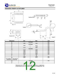
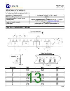
10 (15)

 MAS [ MICRO ANALOG SYSTEMS ]