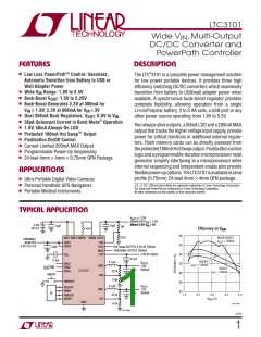
LTC3101
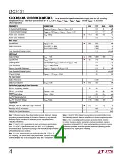
ELECTRICAL CHARACTERISTICS The l denotes the specifications which apply over the full operating
temperature range, otherwise specifications are at TA = 25°C. VUSB1 = VUSB2 = VBAT1 = VBAT2 = 3V and VOUT3 = 3.3V, unless
otherwise noted.
PARAMETER
CONDITIONS
MIN
–11.5
200
TYP
0.1
MAX
5
UNITS
μA
N-Channel Switch Leakage
P-Channel Switch Leakage
Power Good Threshold
Power Good Hysteresis
MAX Output
V
V
V
= V
= V
= V
= 5.5V
OUT3
SW3A,B
SW3A,B
USB1,2
BAT1,2
= 0V, V
= V
= V = 5.5V
OUT3
0.1
10
μA
USB1,2
BAT1,2
l
l
Falling
–8.5
2.5
–5.5
%
FB3
%
Current Limit
V
MAX
= 2.0V
300
mA
Switch Resistance
From BAT2 to MAX
From USB2 to MAX
0.890
0.930
Ω
Ω
Load Dependent Supply Current
LDO Output
1.0
μA/mA
l
l
Output Voltage
I
= 1mA
= 1.0V
1.755
50
1.800
110
0.1
0.9
0.1
12
1.845
V
mA
LDO
Current Limit
V
LDO
Line Regulation
Input Voltage (V
) = 1.8V to 5.5V, I
= 1mA
%
MAX
LDO
Load Regulation
I
= 1mA to 50mA
%
LDO
Reverse Current in Shutdown
Load Dependent Supply Current
Dropout Voltage
V
= V
= 0V, V = 1.8V
LDO
1
μA
BAT1,2
USB1,2
μA/mA
mV
V
= 1.75V, I
= 10mA
LDO
25
MAX
HSO
Hot Swap Output
Switch Resistance
0.730
150
Ω
l
Switch Current Limit
Pushbutton Logic and μP Reset Generator
PBSTAT Deglitching Duration
PBSTAT Low Voltage
RESET Low Voltage
V
= 2.0V
100
15
mA
24
20
ms
mV
mV
μA
V
I
I
= 1mA
= 1mA
50
50
PBSTAT
20
RESET
C
RS
C
RS
Pin Charging Current
Pin Threshold Voltage
0.9
1.0
1.1
V
Rising
1.176
1.200
1.224
CRS
Logic Inputs
l
PWRKEY, PWRON, PWM Input Logic Threshold
PWRKEY Pull-Up Resistance
PWRON Pull-Down Resistance
0.3
0.7
400
4.0
1.0
V
kΩ
MΩ
Note 1: Stresses beyond those listed under Absolute Maximum Ratings
may cause permanent damage to the device. Exposure to any Absolute
Maximum Rating condition for extended periods may affect device
reliability and lifetime.
Note 2: The LTC3101 is guaranteed to meet performance specifications
from 0°C to 85°C. Specifications over the –40°C to 85°C operating
Note 4: The LTC3101 is tested in a proprietary non-switching test mode
that internally connects the error amplifiers in a closed-loop configuration.
Note 5: This IC includes overtemperature protection that is intended
to protect the device during momentary overload conditions. Junction
temperature will exceed 125°C when overtemperature protection is active.
Continuous operation above the specified maximum operating junction
temperature may impair device reliability.
temperature range are ensured by design, characterization and correlation
with statistical process controls.
Note 3: Current measurements are performed when the LTC3101 is
not switching. The current limit values measured in operation will be
somewhat higher due to the propagation delay of the comparators.
3101f
4

 Linear [ Linear ]