LTC3101
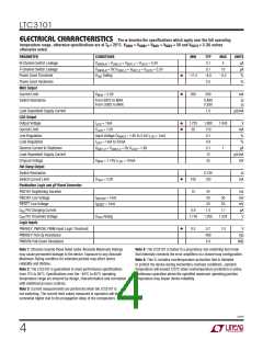
ELECTRICAL CHARACTERISTICS The l denotes the specifications which apply over the full operating
temperature range, otherwise specifications are at TA = 25°C. VUSB1 = VUSB2 = VBAT1 = VBAT2 = 3V and VOUT3 = 3.3V, unless
otherwise noted.
PARAMETER
CONDITIONS
MIN
TYP
MAX
UNITS
%
l
l
Minimum Duty Cycle
0
ENA1 Input Logic Threshold
ENA1 Pull-Down Resistance
N-Channel Switch Resistance
P-Channel Switch Resistance
0.3
0.7
4.0
1.0
V
V
= 3V or V
= 0V
MΩ
Ω
PWRON
PWRKEY
0.34
Battery Powered
USB Powered
0.55
0.58
Ω
Ω
N-Channel Switch Leakage
P-Channel Switch Leakage
Power Good Threshold
V
V
V
= V
= V = 5.5V
BAT1,2
0.1
0.1
–8
5
μA
μA
%
SW1
SW1
FB1
USB1,2
= 0V, V
Falling
= V
= 5.5V
BAT1,2
10
–5
USB1,2
l
l
–11
583
Power Good Hysteresis
Buck Converter 2
2.5
%
Feedback Voltage (FB2 Pin)
Feedback Pin Input Current (FB2 Pin)
P-Channel Current Limit
596
1
609
50
mV
nA
Battery Powered (Note 3)
USB Powered (Note 3)
440
440
540
540
mA
mA
l
l
l
Maximum Duty Cycle
100
%
%
Minimum Duty Cycle
0
ENA2 Input Logic Threshold
ENA2 Pull-Down Resistance
N-Channel Switch Resistance
P-Channel Switch Resistance
0.3
0.7
4.0
1.0
V
V
= 3V or V
= 0V
MΩ
Ω
PWRON
PWRKEY
0.34
Battery Powered
USB Powered
0.55
0.58
Ω
Ω
N-Channel Switch Leakage
P-Channel Switch Leakage
Power Good Threshold
V
SW2
V
SW2
V
FB2
= V
= V = 5.5V
BAT1,2
0.1
0.1
–8
5
μA
μA
%
USB1,2
= 0V, V
Falling
= V
= 5.5V
BAT1,2
10
–5
USB1,2
l
–11
Power Good Hysteresis
2.5
%
Buck-Boost Converter
l
l
Operating Output Voltage
Feedback Voltage (FB3 Pin)
Feedback Pin Input Current (FB3 Pin)
Inductor Current Limit
1.5
5.25
614
50
V
mV
nA
A
584
599
1
BAT or USB Powered (Note 3)
(Note 3)
1.2
1.5
400
450
87
Reverse Inductor Current Limit
Burst Mode Inductor Current Limit
Maximum Duty Cycle
mA
mA
%
(Note 3)
l
l
l
Percentage of Period SW3B is Low in Boost Mode
Percentage of Period SW3A is High in Buck Mode
82
Minimum Duty Cycle
0
%
ENA3 Input Logic Threshold
ENA3 Pull-Down Resistance
N-Channel Switch Resistance
0.3
0.7
4.0
1.0
V
V
= 3V or V
= 0V
MΩ
PWRON
PWRKEY
Switch B (From SW3A to GND)
Switch C (From SW3B to GND)
0.150
0.140
Ω
Ω
P-Channel Switch Resistance
Switch A´ (From BAT2 to SW3A)
Switch A (From USB2 to SW3A)
Switch D (From OUT3 to SW3B)
0.150
0.180
0.195
Ω
Ω
Ω
3101f
3

 Linear [ Linear ]