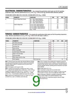
LTC2640
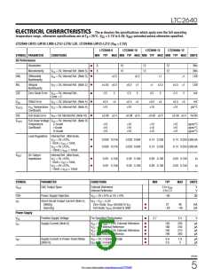
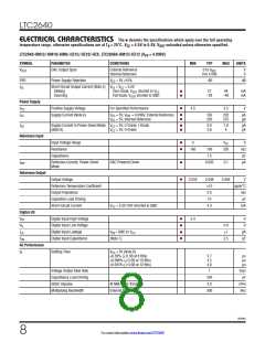
ELECTRICAL CHARACTERISTICS The l denotes the specifications which apply over the full operating
temperature range, otherwise specifications are at TA = 25°C. VCC = 4.5V to 5.5V, VOUT unloaded unless otherwise specified.
LTC2640-HM12/-HM10/-HM8/-HZ12/-HZ10/-HZ8, LTC2640A-HM12/-HZ12 (VFS = 4.096V)
SYMBOL
PARAMETER
CONDITIONS
MIN
TYP
MAX
UNITS
e
n
Output Voltage Noise Density
At f = 1kHz, External Reference
At f = 10kHz, External Reference
At f = 1kHz, Internal Reference
At f = 10kHz, Internal Reference
140
130
210
200
nV√Hz
nV√Hz
nV√Hz
nV√Hz
Output Voltage Noise
0.1Hz to 10Hz, External Reference
0.1Hz to 10Hz, Internal Reference
0.1Hz to 200kHz, External Reference
0.1Hz to 200kHz, Internal Reference,
20
20
650
670
µV
µV
µV
µV
P-P
P-P
P-P
P-P
C
= 0.33µF
REF
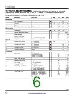
TIMING CHARACTERISTICS
The l denotes the specifications which apply over the full operating temperature
range, otherwise specifications are at TA = 25°C. VCC = 4.5V to 5.5V. (See Figure 1) (Note 7).
LTC2640-HM12/-HM10/-HM8/-HZ12/-HZ10/-HZ8, LTC2640A-HM12/-HZ12 (VFS = 4.096V)
SYMBOL
PARAMETER
CONDITIONS
MIN
4
TYP
MAX
UNITS
ns
l
l
l
l
l
l
l
l
l
l
t
t
t
t
t
t
t
t
t
SDI Valid to SCK Setup
SDI Valid to SCK Hold
SCK High Time
1
4
ns
2
9
ns
3
SCK Low Time
9
ns
4
CS/LD Pulse Width
LSB SCK High to CS/LD High
CS/LD Low to SCK High
CLR Pulse Width
10
7
ns
5
ns
6
7
ns
7
20
7
ns
9
CS/LD High to SCK Pos. Edge
SCK Frequency
ns
10
50% Duty Cycle
50
MHz
Note 1: Stresses beyond those listed under Absolute Maximum Ratings
may cause permanent damage to the device. Exposure to any Absolute
Maximum Rating condition for extended periods may affect device
reliability and lifetime.
Note 5: This IC includes current limiting that is intended to protect the
device during momentary overload conditions. Junction temperature can
exceed the rated maximum during current limiting. Continuous operation
above the specified maximum operating junction temperature may impair
device reliability.
Note 2: All voltages are with respect to GND.
Note 6: Digital inputs at 0V or V
Note 7: Guaranteed by design and not production tested.
.
CC
Note 3: Linearity and monotonicity are defined from code k to code
L
N
N
2 – 1, where N is the resolution and k is given by k = 0.016 • (2 / V ),
L
L
FS
rounded to the nearest whole code. For V = 2.5V and N = 12, k = 26
FS
L
Note 8: Internal Reference mode. DAC is stepped 1/4 scale to 3/4 scale
and 3/4 scale to 1/4 scale. Load is 2k in parallel with 100pF to GND.
Note 9: Temperature coefficient is calculated by dividing the maximum
change in output voltage by the specified temperature range.
and linearity is defined from code 26 to code 4,095. For V = 4.096V
FS
and N = 12, k = 16 and linearity is defined from code 16 to code 4,095.
L
Note 4: Inferred from measurement at code 16 (LTC2640-12), code 4
(LTC2640-10) or code 1 (LTC2640-8), and at full-scale.
Note 10: Full-scale error is determined using the reference voltage
measured at the REF pin.
2640fd
9
For more information www.linear.com/LTC2640

 Linear [ Linear ]