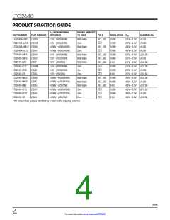
LTC2640
The l denotes the specifications which apply over the full operating
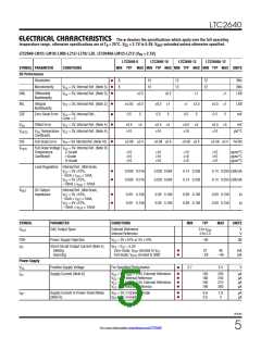
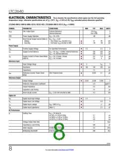
ELECTRICAL CHARACTERISTICS
temperature range, otherwise specifications are at TA = 25°C. VCC = 4.5V to 5.5V, VOUT unloaded unless otherwise specified.
LTC2640-HM12/-HM10/-HM8/-HZ12/-HZ10/-HZ8, LTC2640A-HM12/-HZ12 (VFS = 4.096V)
SYMBOL
PARAMETER
CONDITIONS
MIN
TYP
0 to V
MAX
UNITS
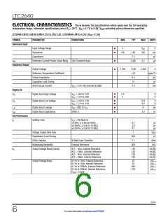
V
OUT
DAC Output Span
External Reference
Internal Reference
V
V
REF
0 to 4.096
PSR
Power Supply Rejection
V
CC
= 5V 10%
–80
dB
I
SC
Short-Circuit Output Current (Note 5)
V
FS
= V = 5.5V
CC
l
l
Sinking
Zero-Scale; V
shorted to V
27
–28
48
–48
mA
mA
OUT
CC
Sourcing
Full-Scale; V
shorted to GND
OUT
Power Supply
l
V
Positive Supply Voltage
Supply Current (Note 6)
For Specified Performance
4.5
5.5
V
CC
l
l
I
CC
V
CC
V
CC
= 5V, V = 4.096V, External Reference
160
200
220
270
µA
µA
REF
= 5V, Internal Reference
l
l
I
SD
Supply Current in Power-Down Mode
(Note 6)
V
CC
V
CC
= 5V, C-Grade, I-Grade
= 5V, H-Grade
0.6
0.6
1.8
4
µA
µA
Reference Input
l
l
Input Voltage Range
Resistance
0
V
V
kΩ
pF
CC
160
190
7.5
220
Capacitance
l
l
I
Reference Current, Power-Down
Mode
DAC Powered Down
0.005
0.1
µA
REF
Reference Output
Output Voltage
2.032
2.048
10
2.064
V
ppm/°C
kΩ
Reference Temperature Coefficient
Output Impedance
0.5
10
Capacitive Load Driving
Short-Circuit Current
µF
V
V
= 5.5V; REF Shorted to GND
4.3
mA
CC
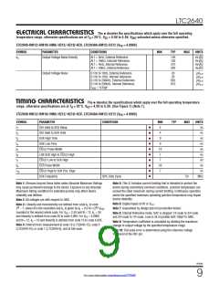
Digital I/O
l
l
l
l
V
Digital Input High Voltage
Digital Input Low Voltage
Digital Input Leakage
2.4
V
V
IH
IL
V
0.8
1
I
LK
= GND to V
µA
pF
IN
CC
C
Digital Input Capacitance
(Note 7)
2.5
IN
AC Performance
t
S
Settling Time
V
= 5V (Note 8)
CC
0.39% ( 1LSB at 8 Bits)
0.098% ( 1LSB at 10 Bits)
0.024% ( 1LSB at 12 Bits)
3.7
4.2
4.6
µs
µs
µs
Voltage Output Slew Rate
Capacitance Load Driving
Glitch Impulse
1
V/µs
pF
500
3.0
300
At Mid-Scale Transition
External Reference
nV•s
kHz
Multiplying Bandwidth
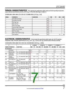
2640fd
8
For more information www.linear.com/LTC2640

 Linear [ Linear ]