LTC2640
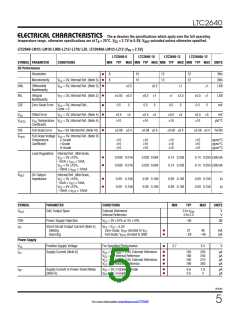
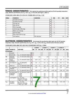
TIMING CHARACTERISTICS The l denotes the specifications which apply over the full operating temperature
range, otherwise specifications are at TA = 25°C. VCC = 2.7V to 5.5V. (See Figure 1) (Note 7).
LTC2640-LM12/-LM10/-LM8/-LZ12/-LZ10/-LZ8, LTC2640A-LM12/-LZ12 (VFS = 2.5V)
SYMBOL
PARAMETER
CONDITIONS
MIN
4
TYP
MAX
UNITS
ns
l
l
l
l
l
l
l
l
l
l
t
t
t
t
t
t
t
t
t
SDI Valid to SCK Setup
SDI Valid to SCK Hold
SCK High Time
1
4
ns
2
9
ns
3
SCK Low Time
9
ns
4
CS/LD Pulse Width
LSB SCK High to CS/LD High
CS/LD Low to SCK High
CLR Pulse Width
10
7
ns
5
ns
6
7
ns
7
20
7
ns
9
CS/LD High to SCK Pos. Edge
SCK Frequency
ns
10
50% Duty Cycle
50
MHz
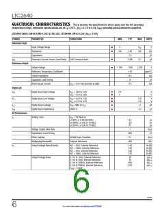
The l denotes the specifications which apply over the full operating
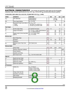
ELECTRICAL CHARACTERISTICS
temperature range, otherwise specifications are at TA = 25°C. VCC = 4.5V to 5.5V, VOUT unloaded unless otherwise specified.
LTC2640-HM12/-HM10/-HM8/-HZ12/-HZ10/-HZ8, LTC2640A-HM12/-HZ12 (VFS = 4.096V)
LTC2640-8
LTC2640-10
LTC2640-12
LTC2640A-12
SYMBOL PARAMETER
DC Performance
Resolution
CONDITIONS
MIN TYP MAX MIN TYP MAX MIN TYP MAX MIN TYP MAX UNITS
l
l
l
8
8
10
10
12
12
12
12
Bits
Bits
LSB
Monotonicity
V
V
= 5V, Internal Ref. (Note 3)
= 5V, Internal Ref. (Note 3)
CC
DNL
INL
Differential
0.5
0.5
5
0.5
1
1
2.5
5
1
1
CC
Nonlinearity
l
l
l
Integral
Nonlinearity
V
= 5V, Internal Ref. (Note 3)
0.05
0.5
0.2
0.5
1
0.5
0.5
LSB
mV
CC
CC
ZSE
Zero-Scale Error
V
= 5V, Internal Ref.,
5
0.5
5
Code = 0
V
V
Offset Error
V
V
= 5V, Internal Ref. (Note 4)
= 5V, Internal Ref. (Note 4)
0.5
10
5
0.5
10
5
0.5
10
5
0.5
10
5
mV
OS
CC
CC
V
Temperature
OS
µV/°C
OSTC
Coefficient
l
FSE
Full-Scale Error
V
CC
= 5V, Internal Ref. (Note 10)
0.08
0.4
0.08 0.4
0.08 0.4
0.08 0.4 %FSR
V
FSTC
Full-Scale Voltage V = 5V, Internal Ref. (Note 9)
CC
Temperature
Coefficient
C-Grade
I-Grade
H-Grade
10
10
10
10
10
10
10
10
10
10
10
10
ppm/°C
ppm/°C
ppm/°C
l
l
Load Regulation
V
= 5V 10%,
0.006 0.01
0.022 0.04
0.09 0.16
0.09 0.16 LSB/mA
CC
Internal Ref. Mid-Scale,
–10mA ≤ I ≤ 10mA
OUT
R
OUT
DC Output
Impedance
V
= 5V 10%,
CC
0.09 0.156
0.09 0.156
0.09 0.156
0.09 0.156
Ω
Internal Ref. Mid-Scale,
–10mA ≤ I ≤ 10mA
OUT
2640fd
7
For more information www.linear.com/LTC2640

 Linear [ Linear ]