LTC2630
OPERATION
INPUT WORD (LTC2630-12)
COMMAND
4 DON'T-CARE BITS
DATA (12 BITS + 4 DON'T-CARE BITS)
C3 C2 C1 C0
X
X
X
X
D11 D10 D9 D8 D7 D6 D5 D4 D3 D2 D1 D0
X
X
X
X
X
X
X
X
X
X
X
MSB
LSB
INPUT WORD (LTC2630-10)
COMMAND
4 DON'T-CARE BITS
DATA (10 BITS + 6 DON'T-CARE BITS)
C3 C2 C1 C0
X
X
X
X
D9 D8 D7 D6 D5 D4 D3 D2 D1 D0
MSB LSB
X
X
INPUT WORD (LTC2630-8)
COMMAND
4 DON'T-CARE BITS
DATA (8 BITS + 8 DON'T-CARE BITS)
C3 C2 C1 C0
X
X
X
X
D7 D6 D5 D4 D3 D2 D1 D0
MSB LSB
X
X
X
X
X
2630 F02
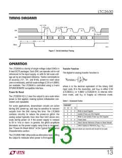
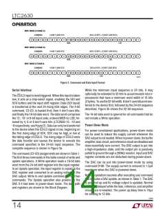
Figure 2. Command and Data Input Format
Serial Interface
While the minimum input sequence is 24 bits, it may
optionally be extended to 32 bits to accommodate micro-
processors that have a minimum word width of 16 bits
(2bytes).Tousethe32-bitwidth,8don’t-carebitsaretrans-
ferred to the device first, followed by the 24-bit sequence
described. Figure 3b shows the 32-bit sequence.
TheCS/LDinputisleveltriggered. Whenthisinputistaken
low, it acts as a chip-select signal, enabling the SDI and
SCK buffers and the input shift register. Data (SDI input)
is transferred at the next 24 rising SCK edges. The 4-bit
command, C3-C0, is loaded first; then 4 don’t-care bits;
and finally the 16-bit data word. The data word comprises
the 12-, 10- or 8-bit input code, ordered MSB-to-LSB, fol-
lowed by 4, 6 or 8 don’t-care bits (LTC2630-12, -10 and
-8 respectively; see Figure 2). Data can only be transferred
to the device when the CS/LD signal is low, beginning on
the first rising edge of SCK. SCK may be high or low at
the falling edge of CS/LD. The rising edge of CS/LD ends
the data transfer and causes the device to execute the
command specified in the 24-bit input sequence. The
complete sequence is shown in Figure 3a.
The 16-bit data word is ignored for all commands that do
not include a Write operation.
Power-Down Mode
For power-constrained applications, power-down mode
can be used to reduce the supply current whenever the
DACoutputisnotneeded.Wheninpower-down,thebuffer
amplifier,biascircuit,andreferencecircuitaredisabledand
draw essentially zero current. The DAC output is put into
a high-impedance state, and the output pin is passively
pulled to ground through a 200kΩ resistor. Input and DAC
register contents are not disturbed during power-down.
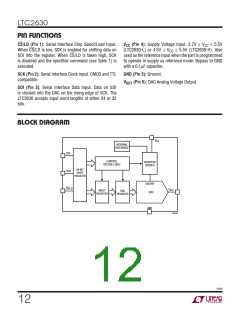
The command (C3-C0) assignments are shown in Table 1.
The first three commands in the table consist of write and
update operations. A Write operation loads a 16-bit data
word from the 24-bit shift register into the input register.
In an Update operation, the input register is copied to the
DAC register and converted to an analog voltage at the
DAC output. Write to and Update combines the first two
commands. The Update operation also powers up the
DAC if it had been in power-down mode. The data path
and registers are shown in the Block Diagram.
The DAC can be put into power-down mode by using
command 0100. The supply current is reduced to 1.5µA
maximum when the DAC is powered down.
Normal operation resumes after executing any command
that includes a DAC update, as shown in Table 1. The DAC
is powered up and its voltage output is updated. Normal
settling is delayed while the bias, reference, and amplifier
circuits are re-enabled. The power up delay time is 18μs
for settling to 12 bits.
2630f
14

 Linear [ Linear ]