LTC2630
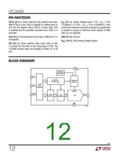
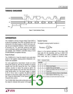
TIMING DIAGRAM
t
1
t
6
t
t
3
t
4
2
SCK
SDI
1
2
3
23
24
t
10
t
t
7
5
CS/LD
2630 F01
Figure 1. Serial Interface Timing
OPERATION
The LTC2630 is a family of single voltage output DACs in
6-lead SC70 packages. Each DAC can operate rail-to-rail
referenced to the input supply, or with its full-scale volt-
age set by an integrated reference. Twelve combinations
of accuracy (12-, 10-, and 8-bit), power-on reset value
(zero or midscale), and full-scale voltage (2.5V or 4.096V)
are available. The LTC2630 is controlled using a 3-wire
SPI/MICROWIRE compatible interface.
Transfer Function
The digital-to-analog transfer function is
k
⎛
⎝
⎞
⎠
VOUT(IDEAL) ⎜
=
V
N ⎟ REF
2
where k is the decimal equivalent of the binary DAC
input code, N is the resolution, and V is either 2.5V
REF
(LTC2630-L) or 4.096V (LTC2630-H) in internal refer-
Power-On Reset
ence mode, and V in Supply as reference mode.
CC
The LTC2630-HZ/-LZ clear the output to zero scale when
power is first applied, making system initialization con-
sistent and repeatable.
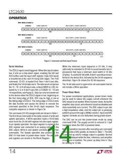
Table 1. Command Codes
Command*
For some applications, downstream circuits are active
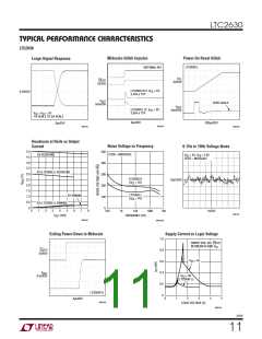
during DAC power-up, and may be sensitive to nonzero
outputs from the DAC during this time. The LTC2630
contains circuitry to reduce the power-on glitch: the
analog output typically rises less than 5mV above zero
scale during power on if the power supply is ramped
to 5V in 1ms or more. In general, the glitch amplitude
decreases as the power supply ramp time is increased.
See “Power-On Reset Glitch” in the Typical Performance
Characteristics section.
C3 C2 C1 C0
0
0
0
0
0
0
0
0
0
1
1
1
0
0
1
0
1
1
0
1
1
0
0
1
Write to Input Register
Update (Power up) DAC Register
Write to and Update (Power up) DAC Register
Power down
Select Internal Reference (Power-on Reset Default)
Select Supply as Reference (V = V
)
CC
REF
*Command codes not shown are reserved and should not be used.
TheLTC2630-HM/-LMprovideanalternativereset,setting
the output to midscale when power is first applied.
2630f
13

 Linear [ Linear ]