LTC2630
PIN FUNCTIONS
CS/LD (Pin 1): Serial Interface Chip Select/Load Input.
When CS/LD is low, SCK is enabled for shifting data on
SDI into the register. When CS/LD is taken high, SCK
is disabled and the specified command (see Table 1) is
executed.
V
(Pin 4): Supply Voltage Input. 2.7V ≤ V ≤ 5.5V
CC CC
(LTC2630-L) or 4.5V ≤ V ≤ 5.5V (LTC2630-H). Also
CC
used as the reference input when the part is programmed
to operate in supply as reference mode. Bypass to GND
with a 0.1μF capacitor.
SCK (Pin 2): Serial Interface Clock Input. CMOS and TTL
compatible.
GND (Pin 5): Ground.
V
OUT
(Pin 6): DAC Analog Voltage Output.
SDI (Pin 3): Serial Interface Data Input. Data on SDI
is clocked into the DAC on the rising edge of SCK. The
LTC2630 accepts input word lengths of either 24 or 32
bits.
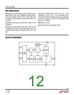
BLOCK DIAGRAM
V
CC
INTERNAL
REFERENCE
SDI
CONTROL
DECODE LOGIC
RESISTOR
DIVIDER
24-BIT
SHIFT
REGISTER
SCK
DACREF
DAC
CS/LD
V
OUT
INPUT
REGISTER
DAC
REGISTER
GND
2630 BD
2630f
12

 Linear [ Linear ]