LTC2309
APPLICATIONS INFORMATION
Overview
Programming the LTC2309
The various modes of operation of the LTC2309 are
The LTC2309 is a low noise, 8-channel, 12-bit succes-
siveapproximationregister(SAR)A/Dconverterwithan
programmed by a 6-bit D word. The SDI input data
IN
2
bits are loaded on the rising edge of SCL during a write
operation,withtheS/Dbitloadedonthefirstrisingedge
and the SLP bit on the sixth rising edge (see Figure 8b
I C compatible serial interface. The LTC2309 includes a
precision internal reference and a configurable 8-chan-
nel analog input multiplexer (MUX). The ADC may be
configuredtoacceptsingle-endedordifferentialsignals
and can operate in either unipolar or bipolar mode. A
sleep mode option is also provided to further reduce
power during inactive periods.
2
in the I C Interface section). The input data word is
defined as follows:
S/D O/S S1 S0 UNI SLP
2
S/D = SINGLE-ENDED/DIFFERENTIAL BIT
O/S = ODD/SIGN BIT
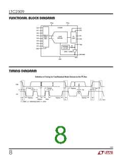
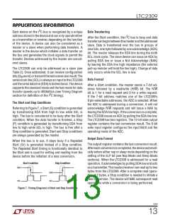
The LTC2309 communicates through a 2-wire I C
compatible serial interface. Conversions are initiated
by signaling a Stop condition after the part has been
successfully addressed for a read/write operation. The
device will not acknowledge (NAK) an external request
until the conversion is finished. After a conversion is
finished, the device is ready to accept a read/write
request. Once the LTC2309 is addressed for a read
operation, the device begins outputting the conversion
result under the control of the serial clock (SCL). There
is no latency in the conversion result. There are 12
bits of output data followed by 4 trailing zeros. Data is
updated on the falling edges of SCL, allowing the user
to reliably latch data on the rising edge of SCL. A write
operation may follow the read operation by using a
Repeat Start or a Stop condition may be given to start
a new conversion. By selecting a write operation, the
S1 = CHANNEL SELECT BIT 1
S0 = CHANNEL SELECT BIT 0
UNI = UNIPOLAR/BIPOLAR BIT
SLP = SLEEP MODE BIT
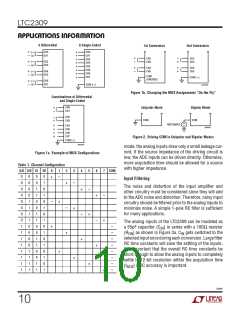
Analog Input Multiplexer
The analog input MUX is programmed by the S/D,
O/S, S1 and S0 bits of the D word. Table 1 lists the
IN
MUX configurations for all combinations of the con-
figuration bits. Figure 1a shows several possible MUX
configurations and Figure 1b shows how the MUX can
be reconfigured from one conversion to the next.
ADC can be programmed with a 6-bit D word. The
IN
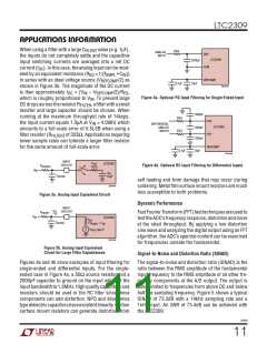
Driving the Analog Inputs
D word configures the MUX and programs various
IN
The analog inputs of the LTC2309 are easy to drive.
Eachoftheanaloginputscanbeusedasasingle-ended
input relative to the COM pin (CH0-COM, CH1-COM,
etc.) or in differential input pairs (CH0 and CH1, CH2
and CH3, CH4 and CH5, CH6 and CH7). Figure 2 shows
how to drive COM for single-ended inputs in unipolar
and bipolar modes. Regardless of the MUX configura-
tion, the “+” and “–“ inputs are sampled at the same
instant. Any unwanted signal that is common to both
inputs will be reduced by the common mode rejection
of the sample-and-hold circuit. The inputs draw only
onesmallcurrentspikewhilechargingthesample-and-
holdcapacitorsduringtheacquiremode. Inconversion
modes of operation of the ADC.
During a conversion, the internal 12-bit capacitive
chargeredistributionDACoutputissequencedthrough
asuccessiveapproximationalgorithmbytheSARstart-
ing from the most significant bit (MSB) to the least
significantbit(LSB). Thesampledinputissuccessively
compared with binary weighted charges supplied by
the capacitive DAC using a differential comparator. At
the end of a conversion, the DAC output balances the
analog input. The SAR contents (a 12-bit data word)
that represent the sampled analog input are loaded into
12 output latches that allow the data to be shifted out
2
via the I C interface.
2309f
9

 Linear [ Linear ]